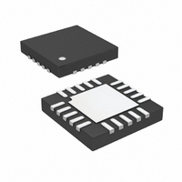
LTC6601CUF-2#TRPBF Linear Technology, LTC6601CUF-2#TRPBF Datasheet - Page 3

LTC6601CUF-2#TRPBF
Manufacturer Part Number
LTC6601CUF-2#TRPBF
Description
IC FILTER/ADC DVR LP LD 20-QFN
Manufacturer
Linear Technology
Datasheet
1.LTC6601CUF-2PBF.pdf
(40 pages)
Specifications of LTC6601CUF-2#TRPBF
Frequency - Cutoff Or Center
27MHz
Number Of Filters
3
Max-order
2nd
Voltage - Supply
2.7 V ~ 5.25 V
Mounting Type
Surface Mount
Package / Case
20-QFN
Lead Free Status / RoHS Status
Lead free / RoHS Compliant
Filter Type
-
Available stocks
Company
Part Number
Manufacturer
Quantity
Price
Part Number:
LTC6601CUF-2#TRPBFLTC6601CUF-2#PBF
Manufacturer:
Linear Technology
Quantity:
135
DC ELECTRICAL CHARACTERISTICS
temperature range, otherwise specifi cations are at T
I
(V
Figure 1.
SYMBOL
ΔR
I
I
V
CMRRI
(Notes 9, 14)
CMRRO
(Notes 9, 14)
PSRR (Note 10)
PSRRCM (Note 10) Common Mode Power Supply Rejection Ratio
g
BAL
V
ΔV
V
R
V
B
OS
LOAD
cm
INCM
OSCM
OUTCMR
MID
INVOCM
OUT
(Note 7)
OSCM
IN
(Note 7)
(Note 14)
+
= 0, R
(Note 8)
/ΔT
+ V
(Note 8)
OUT
BAL
–
)/2. V
= 100k. The fi lter is confi gured for a gain of 1 unless otherwise noted. V
PARAMETER
Input Resistance Match, BIAS = V
Single Ended Input Resistance, Pin 2 or Pin 4 V
Internal Amplifi er Input Bias
Internal Amplifi er Input Offset
Input Signal Common Mode Range
(V
BIAS = V
BIAS = V
BIAS Pin Floating, V
BIAS Pin Floating, V
Input Common Mode Rejection Ratio
(Amplifi er Input Referred) ΔV
ΔV
Output Common Mode Rejection Ratio
(Amplifi er Input Referred) ΔV
ΔV
Power Supply Rejection Ratio
(Amplifi er Input Referred) ΔV
BIAS Pin Floating
BIAS = V
(ΔV
Common Mode Gain (ΔV
ΔV
Common Mode Gain Error = 100 • (g
ΔV
Output Balance (ΔV
Single-Ended Input
Differential Input
Common Mode Offset Voltage
(V
Common Mode Offset Voltage Drift
(V
Output Signal Common Mode Range
(Voltage Range for the V
Input Resistance, V
Voltage at the V
INCM
INP
OUTCM
OUTCM
INCM
OCM
OCM
OCM
S
/ΔV
+ V
is defi ned as (V
= 1V
= 2V
= 2V
= 2.5V
+
+
+
OSCM
INM
– V
– V
, V
, V
)/2
OCM
OCM
OCM
OCM
)
OCM
)
)
= 2.5V
= 1.5V
OCM
OUTCM
OCM
OCM
PIn
Pin
OCM
= 2.5V
= 1.5V
OUTCM
INP
/ΔV
Pin)
+ V
INCM
OCM
S
OUTDIFF
/ΔV
/ΔV
INM
/ΔV
+
/ΔV
OSDIFF
OCM
)
)/2. V
cm
OSDIFF
OSDIFF
A
)
– 1)
= 25°C. V
OUTDIFF
CONDITIONS
V
V
V
V
V
V
V
V
V
V
V
V
V
ΔV
V
V
V
V
V
V
V
V
V
V
V
V
S
S
S
S
S
S
S
S
S
S
S
S
S
S
S
S
S
S
S
S
S
S
S
S
S
S
OUTDIFF
= 3V
= 2.7V to 5V
= 2.7V to 5V
= 5V
= 3V
= 5V
= 3V
= 5V
= 5V
= 2.7V to 5V
= 2.7V to 5V
= 2.7V to 5V
= 5V
= 5V
= 5V
= 5V
= 2.7V to 5V
= 2.7V to 5V
= 2.7V to 5V
= 2.7V to 5V
= 3V
= 5V
= 3V
= 5V
= 3V
= 3V
+
is defi ned as (V
= 3V, V
The
= 2V
l
denotes the specifi cations which apply over the full operating
–
= 0V, V
BIAS = Floating
BIAS = V
BIAS = Floating
BIAS = V
BIAS = Floating
BIAS = V
BIAS = Floating
BIAS = V
BIAS Pin Floating
BIAS Pin Floating
BIAS = V
BIAS = V
OUT
INCM
+
– V
= V
+
+
+
+
+
+
S
OUT
OCM
is defi ned as (V
–
). V
= mid-supply, BIAS tied to V
INDIFF
l
l
l
l
l
l
l
l
l
l
l
l
l
l
l
l
l
l
l
l
l
l
l
l
l
is defi ned as (V
1.475
MIN
–25
–50
1.1
1.1
1.1
1.1
58
58
40
0
0
0
0
5
+
– V
–
). V
LTC6601-2
±0.25
–12.5
±0.3
TYP
–25
–58
–62
±15
±15
1.5
±1
±1
74
70
94
81
51
20
20
1
7
OUTCM
INP
1.525
is defi ned as
– V
MAX
±1.0
+
±10
–40
–40
±30
±30
4.7
1.7
4.8
1.8
1.8
1.7
±5
0
0
4
4
9
or fl oating,
INM
). See
UNITS
μV/°C
μV/°C
66012f
3
V/V
mV
mV
kΩ
μA
μA
μA
μA
dB
dB
dB
dB
dB
dB
dB
%
Ω
V
V
V
V
V
V
V
V
V


