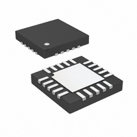
LTC6601CUF-2#TRPBF Linear Technology, LTC6601CUF-2#TRPBF Datasheet - Page 31

LTC6601CUF-2#TRPBF
Manufacturer Part Number
LTC6601CUF-2#TRPBF
Description
IC FILTER/ADC DVR LP LD 20-QFN
Manufacturer
Linear Technology
Datasheet
1.LTC6601CUF-2PBF.pdf
(40 pages)
Specifications of LTC6601CUF-2#TRPBF
Frequency - Cutoff Or Center
27MHz
Number Of Filters
3
Max-order
2nd
Voltage - Supply
2.7 V ~ 5.25 V
Mounting Type
Surface Mount
Package / Case
20-QFN
Lead Free Status / RoHS Status
Lead free / RoHS Compliant
Filter Type
-
Available stocks
Company
Part Number
Manufacturer
Quantity
Price
Part Number:
LTC6601CUF-2#TRPBFLTC6601CUF-2#PBF
Manufacturer:
Linear Technology
Quantity:
135
COMPLEX FILTER CONFIGURATIONS
A Modifi ed 2nd Order Lowpass Filter Topology
The basic fi lter topology of Figure 3 can be modifi ed as
shown in Figure 13. The Figure 13 circuit includes an
impedance path between the two summing nodes (the
circuit nodes common to resistors R1, R2 and R3). A
resistor and/or a capacitor connection between the sum-
ming nodes provide even more fl exibility, and enhance
the fi lter design options (the f
in Figure 13 reduce to equations of Figure 3 if C3 is zero
and R4 is infi nite).
The modifi ed second order fi lter topology provides for
setting the Q value (with R4) without changing the f
value and increasing the passband gain to greater than
one without changing the Q value (in the Q equation of
Figure 13 the value of Q does not change if the value of
the [1 + GAIN + 2(R2/R4)] denominator factor does not
change). Using R4 to set the Q value allows the option
to design the –3dB frequency (f
and the f
ies in a second order lowpass function (refer to the f
equation of Figure 13).
APPLICATIONS INFORMATION
O
value is constant then the f
O
3dB
and Q equations shown
). If the Q value varies
3dB
frequency var-
3dB
O
Figures 14 to 17 show additional circuits highlighting the
use of R4 or C3 in the modifi ed second order cicuit to
set the f
24.6MHz respectively.
The design procedure for a specifi ed f
as follows:
1 Using the chosen C1, C2 and C3 values calculate the
2. Using f
3. Calculate the R4 value using the Q value of step 3.
4. Calculate the required external resistor R
Note: The modifi ed second order fi lter topology requires
the use of at least two of the three input resistor pairs (two
of the three 400Ω, 200Ω and 100Ω pairs).
f
Q value.
the R4 value in step 3. Example, in Figure 14 the Q
value for f
is 350Ω, the R4A and R4B resistors are the internal
100Ω and the R
+ R4B)].
O
value.
3dB
O
of step 1 and the specifi ed f
frequency to 13MHz, 19MHz, 22.7MHz and
3dB
= 5MHz is 0.54, the required R4 resistor
EXT
resistor is 150Ω [R
LTC6601-2
3dB
3dB
EXT
frequency is
calculate the
EXT
= R4 – (R4A
value for
31
66012f


