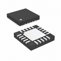
LTC6601CUF-2#TRPBF Linear Technology, LTC6601CUF-2#TRPBF Datasheet - Page 20

LTC6601CUF-2#TRPBF
Manufacturer Part Number
LTC6601CUF-2#TRPBF
Description
IC FILTER/ADC DVR LP LD 20-QFN
Manufacturer
Linear Technology
Datasheet
1.LTC6601CUF-2PBF.pdf
(40 pages)
Specifications of LTC6601CUF-2#TRPBF
Frequency - Cutoff Or Center
27MHz
Number Of Filters
3
Max-order
2nd
Voltage - Supply
2.7 V ~ 5.25 V
Mounting Type
Surface Mount
Package / Case
20-QFN
Lead Free Status / RoHS Status
Lead free / RoHS Compliant
Filter Type
-
Available stocks
Company
Part Number
Manufacturer
Quantity
Price
Part Number:
LTC6601CUF-2#TRPBFLTC6601CUF-2#PBF
Manufacturer:
Linear Technology
Quantity:
135
APPLICATIONS INFORMATION
LTC6601-2
Table 1 lists the amplifi er input referred noise for the
LTC6601-2. Tables 2 to10 list the noise referred to the input
pins of the IC for common confi gurations of the LTC6601-2.
To determine the spot noise at the output, simply multiply
the noise by the Gain = R2/R1. To estimate the integrated
noise at the output, multiply the noise by the gain, and the
square root of the noise bandwidth. The noise bandwidth
depends on the fi lter confi guration. For Figure 2, the noise
bandwidth is 100MHz, or approximately 7 times the fi lter
bandwidth. Improvements in SNR can be made by adding
an additional RC fi lter at the output to band limit wide band
noise before feeding ADCs. See the section “Interfacing
the LTC6601 to ADC Converters” for more detail.
Table 1. Amplifi er (Input Referred) Noise Characteristics for the
LTC6601-2
LAYOUT CONSIDERATIONS
Because the LTC6601 is a very high speed amplifi er, it is
sensitive to both stray capacitance and stray inductance.
It is critical that close attention be paid to supply bypass-
ing. For single supply applications, it is recommended
that a high quality 0.1μF surface mount ceramic bypass
capacitor be placed between Pins 14 and 13 with direct
short connections. Pin 13 and the Exposed Pad, Pin 21,
should be tied directly to a low impedance ground plane
with minimal routing. For dual (split) power supplies, it
is recommended that an additional high quality, 0.1μF
20
nV/√Hz
BIAS PIN PULLED TO V
4.7
e
ni
pA/√Hz
i
3
n
+
nV/√Hz
5.2
e
BIAS PIN FLOATING
ni
Figure 5. Differential Noise Model of the LTC6601
e
e
nR1
nR1
*
*
2
2
R1
R1
pA/√Hz
2.1
i
n
e
e
nR3
nR3
*
*
2
2
I
I
n
n
R3
R3
+ 2
– 2
ceramic capacitor be used to bypass pin V
and V
ing large differential loads (<200Ω), additional bypass
capacitance may be needed between V
mal performance. Note that small geometry (e.g., 0603)
surface mount ceramic capacitors have a much higher
self resonant frequency than capacitors with leads, and
perform best in high speed applications.
The V
quality ceramic capacitor whose value exceeds 0.01μF ,
with direct, short connections. In split supply applications,
the V
hardwired to ground. Be careful not to violate the output
common mode range specifi cations for the V
Stray parasitic capacitances to unused component pins
that set up the fi lter’s characteristics, should be kept to an
absolute minimum. This prevents deviations from the ideal
frequency response. An ideal layout technique would be to
remove the solder pads for the unused component pins,
and strip away the ground plane underneath these pins to
lower capacitance to an absolute minimum. Floating unused
component pins which set up the fi lter characteristics will
not reduce the reliability of the LTC6601.
At the output, always keep in mind the differential nature of
the LTC6601, and that it is critical that the load impedances
seen by both outputs (stray or intended), should be as bal-
anced and symmetric as possible. This will help preserve
the natural balance of the LTC6601, which minimizes the
generation of even order harmonics and preserves the
rejection of common mode signals and noise.
e
*
ni
e
e
2
nR2
nR2
*
*
OCM
2
2
OCM
–
+
–
to ground, again with minimal routing. For driv-
R2
R2
pin can be either bypassed to ground or directly
pin should be bypassed to ground with a high
66012 F05
e
no
2
+
and V
+
OCM
to ground
–
for opti-
pin.
66012f


