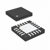
LTC6601CUF-2#TRPBF Linear Technology, LTC6601CUF-2#TRPBF Datasheet - Page 21

LTC6601CUF-2#TRPBF
Manufacturer Part Number
LTC6601CUF-2#TRPBF
Description
IC FILTER/ADC DVR LP LD 20-QFN
Manufacturer
Linear Technology
Datasheet
1.LTC6601CUF-2PBF.pdf
(40 pages)
Specifications of LTC6601CUF-2#TRPBF
Frequency - Cutoff Or Center
27MHz
Number Of Filters
3
Max-order
2nd
Voltage - Supply
2.7 V ~ 5.25 V
Mounting Type
Surface Mount
Package / Case
20-QFN
Lead Free Status / RoHS Status
Lead free / RoHS Compliant
Filter Type
-
Available stocks
Company
Part Number
Manufacturer
Quantity
Price
Part Number:
LTC6601CUF-2#TRPBFLTC6601CUF-2#PBF
Manufacturer:
Linear Technology
Quantity:
135
INTERFACING THE LTC6601 TO ADC CONVERTERS
The LTC6601’s rail-to-rail differential output and adjustable
output common mode voltage make the LTC6601 ideal
for interfacing to low voltage, single supply, differential
input ADCs. The sampling process of ADCs creates a
sampling transient that is caused by the switching-in
of the ADC sampling capacitor. The switching-in of this
sampling capacitor momentarily “shorts” the output of the
amplifi er as charge is transferred between amplifi er and
sampling capacitor. The amplifi er must recover and settle
from this load transient before this acquisition period has
ended, for a valid representation of the input signal. The
LTC6601 will settle much more quickly from these peri-
odic load impulses than it does from a 2V input step, but
it is a good idea to add an RC network after the outputs
of the LTC6601 to decouple the sampling transient of the
ADC (See Figure 6). The capacitance of the decoupling
network serves to provide the bulk of the charge during
the sampling process, while the two resistors of the fi lter
network are used to dampen and attenuate any transient
induced by the ADC. The ADC’s sampling bandwidth will
APPLICATIONS INFORMATION
V
IN
+
–
BIAS
1μF
1
2
3
4
5
LTC6601-2
20
6
19
7
18
8
+
–
Figure 6. Interfacing the LTC6601 to A/D Converters
17
9
16
10
15
14
13
12
11
V
V
OUT
OUT
0.1μF
–
+
often be much greater than that of the LTC6601, so hav-
ing this discrete RC fi lter will give the additional benefi t
of band limiting broadband output noise.
The selection of the RC time constant is trial and error
for a given ADC, but the following guidelines are recom-
mended. Choose an RC pole frequency greater than the
cutoff frequency of the LTC6601. 80MHz RC fi lters are
good for fi ltering broadband noise. Lower frequency RC
fi lters improve SNR at the expense of settling time. The
resistors in the decoupling network should be at least 25Ω.
Too much resistance in the decoupling network leaves
insuffi cient settling time and will create a voltage divider
between the dynamic input impedance of the ADC and the
decoupling resistors. Using insuffi cient resistance might
prevent proper dampening of the load transient caused by
the sampling process, and prolong the time required for
settling. In 16-bit applications, this will typically require
a minimum of 11 RC time constants. It is recommended
that the capacitor is chosen with low dielectric absorption
(such as a C0G multilayer ceramic capacitor).
3V
1μF
V
10nF
OCM
t = R • (C1 + 2 • C2)
R
R
C2
C1
C1
66012 F06
A
A
IN
IN
+
–
V
CM
2.2μF
CONTROL
GND
LTC6601-2
D15
D0
•
•
1μF
21
1μF
3.3V
66012f


