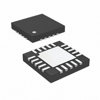
LTC6601CUF-2#TRPBF Linear Technology, LTC6601CUF-2#TRPBF Datasheet - Page 4

LTC6601CUF-2#TRPBF
Manufacturer Part Number
LTC6601CUF-2#TRPBF
Description
IC FILTER/ADC DVR LP LD 20-QFN
Manufacturer
Linear Technology
Datasheet
1.LTC6601CUF-2PBF.pdf
(40 pages)
Specifications of LTC6601CUF-2#TRPBF
Frequency - Cutoff Or Center
27MHz
Number Of Filters
3
Max-order
2nd
Voltage - Supply
2.7 V ~ 5.25 V
Mounting Type
Surface Mount
Package / Case
20-QFN
Lead Free Status / RoHS Status
Lead free / RoHS Compliant
Filter Type
-
Available stocks
Company
Part Number
Manufacturer
Quantity
Price
Part Number:
LTC6601CUF-2#TRPBFLTC6601CUF-2#PBF
Manufacturer:
Linear Technology
Quantity:
135
DC ELECTRICAL CHARACTERISTICS
LTC6601-2
SYMBOL
V
I
V
I
I
V
V
V
R
V
t
t
temperature range, otherwise specifi cations are at T
I
(V
Figure 1.
4
SC
S
SHDN
ON
OFF
LOAD
OUT
S
BIASSD
BIASLP
BIASHP
BIAS
BIAS
OUT
+
= 0, R
(Note 13)
+ V
OUT
BAL
–
)/2. V
= 100k. The fi lter is confi gured for a gain of 1 unless otherwise noted. V
PARAMETER
Output Voltage, High, Either Output Pin
(Note 11)
Output Voltage, Low, Either Output Pin
(Note 11)
Output Short-Circuit Current,
Either Output Pin (Note 12)
Supply Voltage Range
Supply Current, BIAS Pin Floating
Supply Current, BIAS Pin Tied to V
Supply Current, BIAS Pin Tied to V
BIAS Input Pin Range for Shutdown
BIAS Input for Low Power Operation
BIAS Input for High Performance Operation
BIAS Input Resistance
BIAS Float Voltage
Turn-On Time
Turn-Off Time
INCM
is defi ned as (V
INP
+ V
INM
+
–
)/2. V
A
= 25°C. V
OUTDIFF
CONDITIONS
V
V
V
V
V
V
V
V
V
V
V
V
V
V
V
V
V
V
V
V
V
V
V
V
V
V
V
V
V
V
V
V
V
V
V
V
V
V
V
V
V
V
S
S
S
S
S
S
S
S
S
S
S
S
S
S
S
S
S
S
S
S
S
S
S
S
S
S
S
S
S
S
S
S
S
S
S
S
S
S
S
S
S
S
= 3V, I
= 3V, I
= 3V, I
= 5V, I
= 5V, I
= 5V, I
= 3V, I
= 3V, I
= 3V, I
= 5V, I
= 5V, I
= 5V, I
= 3V, I
= 3V, I
= 3V, I
= 5V, I
= 5V, I
= 5V, I
= 3V, I
= 3V, I
= 3V, I
= 5V, I
= 5V, I
= 5V, I
= 3V
= 5V
= 2.7V
= 3V
= 5V
= 2.7V
= 3V
= 5V
= 2.7V
= 3V
= 5V
= 2.7V to 5V
= 2.7V to 5V
= 2.7V to 5V
= 2.7V to 5V
= 2.7V to 5V
= 3V, V
= 3V, V
+
is defi ned as (V
= 3V, V
The
L
L
L
L
L
L
L
L
L
L
L
L
L
L
L
L
L
L
L
L
L
L
L
L
SHDN
SHDN
= 0mA,
= –5mA, BIAS Pin Floating
= –20mA, BIAS Pin Floating
= 0mA,
= –5mA, BIAS Pin Floating
= –20mA, BIAS Pin Floating
= 0mA
= –5mA BIAS = V
= –20mA BIAS = V
= 0mA
= –5mA BIAS = V
= –20mA BIAS = V
= 0mA, BIAS Pin Floating
= 5mA, BIAS Pin Floating
= 20mA, BIAS Pin Floating
= 0mA, BIAS Pin Floating
= 5mA, BIAS Pin Floating
= 20mA, BIAS Pin Floating
= 0mA
= 5mA
= 20mA BIAS = V
= 0mA
= 5mA
= 20mA BIAS = V
l
denotes the specifi cations which apply over the full operating
–
= 0V, V
= 0.25V to 3V
= 3V to 0.25V
BIAS Pin Floating
BIAS Pin Floating
BIAS = V
BIAS = V
BIAS = V
BIAS = V
BIAS = V
BIAS = V
OUT
INCM
+
– V
= V
+
+
+
+
+
+
+
+
+
+
+
+
S
OUT
OCM
is defi ned as (V
–
). V
= mid-supply, BIAS tied to V
INDIFF
l
l
l
l
l
l
l
l
l
l
l
l
l
l
l
l
l
l
l
l
l
l
l
l
l
l
l
l
l
l
l
l
l
l
l
l
l
l
l
l
l
V
V
V
–
is defi ned as (V
–
–
MIN
±45
±60
100
+ 1.05
2.7
V
+ 1.0
+ 2.3
+
–
– V
–
). V
15.8
16.7
32.2
0.45
0.65
1.15
V
TYP
240
290
470
370
430
650
245
285
415
350
390
550
110
120
170
150
170
225
120
135
195
175
200
270
±65
±90
150
400
400
0.4
16
32
33
–
OUTCM
+
INP
V
V
V
–
is defi ned as
1100
1000
–
–
– V
MAX
5.25
23.5
24.5
41.5
+
450
525
850
675
775
450
525
750
625
700
200
225
300
270
300
400
225
250
350
325
360
475
200
1.1
1.8
+ 1.25
23
41
43
V
+ 0.4
+ 1.5
1
or fl oating,
+
INM
). See
UNITS
66012f
mV
mV
mV
mV
mV
mV
mV
mV
mV
mV
mV
mV
mV
mV
mV
mV
mV
mV
mV
mV
mV
mV
mV
mV
mA
mA
mA
mA
mA
mA
mA
mA
mA
mA
mA
kΩ
ns
ns
V
V
V
V
V


