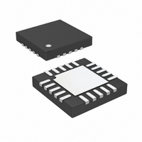
LTC6601CUF-2#TRPBF Linear Technology, LTC6601CUF-2#TRPBF Datasheet - Page 2

LTC6601CUF-2#TRPBF
Manufacturer Part Number
LTC6601CUF-2#TRPBF
Description
IC FILTER/ADC DVR LP LD 20-QFN
Manufacturer
Linear Technology
Datasheet
1.LTC6601CUF-2PBF.pdf
(40 pages)
Specifications of LTC6601CUF-2#TRPBF
Frequency - Cutoff Or Center
27MHz
Number Of Filters
3
Max-order
2nd
Voltage - Supply
2.7 V ~ 5.25 V
Mounting Type
Surface Mount
Package / Case
20-QFN
Lead Free Status / RoHS Status
Lead free / RoHS Compliant
Filter Type
-
Available stocks
Company
Part Number
Manufacturer
Quantity
Price
Part Number:
LTC6601CUF-2#TRPBFLTC6601CUF-2#PBF
Manufacturer:
Linear Technology
Quantity:
135
ABSOLUTE MAXIMUM RATINGS
LTC6601-2
(Note 1)
Total Supply Voltage (V
Input Voltage (Any Pin) (Note 2) ..V
Input Current (V
Input Current (Pins 1, 5) (Note 2) ........................±20mA
Input Current (Pins 2, 4) (Note 2) ........................±30mA
Input Current (Pins 6, 20) (Note 2) ......................±15mA
Input Current (Pins 7, 8, 9, 10, 16, 17, 18, 19)
(Note 2) ................................................................±10mA
Output Short-Circuit Duration (Note 3) ............ Indefi nite
Operating Temperature Range (Note 4)....–40°C to 85°C
Specifi ed Temperature Range (Note 5) ....–40°C to 85°C
Junction Temperature ........................................... 150°C
Storage Temperature Range ...................–65°C to 150°C
ORDER INFORMATION
LEAD FREE FINISH
LTC6601CUF-2#PBF
LTC6601IUF-2#PBF
Consult LTC Marketing for parts specifi ed with wider operating temperature ranges. *The temperature grade is identifi ed by a label on the shipping container.
For more information on lead free part marking, go to:
For more information on tape and reel specifi cations, go to:
DC ELECTRICAL CHARACTERISTICS
SYMBOL
V
ΔV
(Note 6)
R
2
temperature range, otherwise specifi cations are at T
I
(V
Figure 1.
LOAD
OSDIFF
IN
OUT
OSDIFF
(Note 14)
+
= 0, R
(Note 6)
+ V
/ΔT
OUT
BAL
–
)/2. V
= 100k. The fi lter is confi gured for a gain of 1 unless otherwise noted. V
PARAMETER
Amplifi er Differential Offset Voltage (Input
Referred)
Ampifi er Differential Offset Voltage Drift
(Input Referred)
Input Resistance, BIAS = V
Single Ended Input Resistance, Pin 2 or Pin 4
Differential Input Resistance
OCM
INCM
, BIAS) ..................................±10mA
TAPE AND REEL
LTC6601CUF-2#TRPBF
LTC6601IUF-2#TRPBF
is defi ned as (V
+
to V
–
) ...............................5.5V
INP
+
+
+ 0.3V to V
+ V
http://www.linear.com/leadfree/
INM
PART MARKING*
66012
66012
)/2. V
http://www.linear.com/tapeandreel/
A
= 25°C. V
–
OUTDIFF
–0.3V
CONDITIONS
V
V
V
V
S
S
S
S
= 2.7V to 5.25V, BIAS = Floating
= 2.7V to 5.25V
= 3V
= 3V
+
is defi ned as (V
= 3V, V
The
PIN CONFIGURATION
l
denotes the specifi cations which apply over the full operating
–
PACKAGE DESCRIPTION
20-Lead (4mm × 4mm) Plastic QFN
20-Lead (4mm × 4mm) Plastic QFN
= 0V, V
BIAS = V
OUT
INCM
EXPOSED PAD (PIN 21) IS V
+
BIAS
IN2
IN1
IN1
IN2
– V
= V
+
+
+
–
–
T
S
20-LEAD (4mm 4mm) PLASTIC QFN
OUT
JMAX
OCM
1
2
3
4
5
is defi ned as (V
–
= 150°C, θ
). V
= mid-supply, BIAS tied to V
20 19 18 17 16
6
INDIFF
l
l
UF PACKAGE
TOP VIEW
7
JA
21
= 37°C/W, θ
8
–
is defi ned as (V
, MUST BE SOLDERED TO PCB
MIN
9 10
+
– V
JC
–
). V
= 4.3°C/W
±0.25
±0.25
TEMPERATURE RANGE
0°C to 70°C
–40°C to 85°C
TYP
133
200
15
14
13
12
11
1
OUTCM
OUT
V
V
V
OUT
+
–
OCM
INP
–
+
±1.25
is defi ned as
MAX
– V
+
±2
or fl oating,
INM
). See
UNITS
μV/°C
66012f
mV
mV
Ω
Ω


