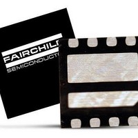
FDMC8200S Fairchild Semiconductor, FDMC8200S Datasheet

FDMC8200S
Specifications of FDMC8200S
Available stocks
Related parts for FDMC8200S
FDMC8200S Summary of contents
Page 1
... Package Marking and Ordering Information Device Marking Device FDMC8200S FDMC8200S ©2011 Fairchild Semiconductor Corporation FDMC8200S Rev.C4 ® MOSFET General Description This device includes two specialized N-Channel MOSFETs in a due power33(3mm X 3mm MLP) package. The switch node has = 6 A been internally connected to enable easy placement and routing D of synchronous buck converters ...
Page 2
... Fall Time f Q Total Gate Charge g(TOT) Q Total Gate Charge g(TOT) Q Gate to Source Charge gs Q Gate to Drain “Miller” Charge gd ©2011 Fairchild Semiconductor Corporation FDMC8200S Rev. 25°C unless otherwise noted J Test Conditions = 250 μ 1mA 250 μA, referenced to 25°C I ...
Page 3
... Q1 mH Vgs = 10V, Vdd = 27V, 100% test mH Q2 100% test mH 3 N-ch device, the negative Vgs rating is for low duty cycle pulse ocurrence only. No continuous rating is implied. ©2011 Fairchild Semiconductor Corporation FDMC8200S Rev. 25°C unless otherwise noted J Test Conditions V ...
Page 4
... Figure 3. Normalized On Resistance vs Junction Temperature 40 μ PULSE DURATION = 80 s DUTY CYCLE = 0.5% MAX 150 2.0 2.5 3 GATE TO SOURCE VOLTAGE (V) GS Figure 5. Transfer Characteristics ©2011 Fairchild Semiconductor Corporation FDMC8200S Rev. 25°C unless otherwise noted μ s 2.0 2.5 3.0 100 50 75 100 125 150 0.01 ...
Page 5
... R = 125 C 180 C/W θ JA θ 0.01 0.001 0.01 0.1 1 0.01 0 DRAIN to SOURCE VOLTAGE ( DRAIN to SOURCE VOLTAGE (V) DS Figure 11. Forward Bias Safe Operating Area ©2011 Fairchild Semiconductor Corporation FDMC8200S Rev. 25°C unless otherwise noted J 1000 100 0 Figure 10. 100 100 us 100 100 100 ms ...
Page 6
... Typical Characteristics (Q1 N-Channel) 2 DUTY CYCLE-DESCENDING ORDER 0.5 0.2 0.1 0.05 0.1 0.02 0.01 SINGLE PULSE 0.01 R θ JA 0.003 - Figure 13. Junction-to-Ambient Transient Thermal Response Curve ©2011 Fairchild Semiconductor Corporation FDMC8200S Rev. 25°C unless otherwise noted 180 C RECTANGULAR PULSE DURATION (sec NOTES: DUTY FACTOR ...
Page 7
... PULSE DURATION = 80 s DUTY CYCLE = 0.5% MAX 150 1.0 1.5 2.0 2 GATE TO SOURCE VOLTAGE (V) GS Figure 18. Transfer Characteristics ©2011 Fairchild Semiconductor Corporation FDMC8200S Rev. °C unless otherwise noted μ s 1.0 1.5 Figure 15. Normalized on-Resistance vs Drain 100 100 125 150 0.1 ...
Page 8
... Figure 22. Unclamped Inductive Switching Capability THIS AREA IS LIMITED BY r DS(on) SINGLE PULSE 0 MAX RATED 125 C/W θ 0.01 0.01 0 DRAIN to SOURCE VOLTAGE (V) DS Figure 24. Forward Bias Safe Operating Area ©2011 Fairchild Semiconductor Corporation FDMC8200S Rev. 25°C unless otherwise noted 100 100 100 ...
Page 9
... Typical Characteristics (Q2 N-Channel) 2 DUTY CYCLE-DESCENDING ORDER 0.5 0.2 0.1 0.1 0.05 0.02 0.01 0.01 SINGLE PULSE R θ ( Note 1b 0.001 - Figure 26. Junction-to-Ambient Transient Thermal Response Curve ©2011 Fairchild Semiconductor Corporation FDMC8200S Rev. °C unless otherwise noted 125 C RECTANGULAR PULSE DURATION (sec NOTES: DUTY FACTOR ...
Page 10
... TIME (ns) Figure 27. FDMC8200S SyncFET body diode reverse recovery characteristic ©2011 Fairchild Semiconductor Corporation FDMC8200S Rev.C4 (continued) Schottky barrier diodes exhibit significant leakage at high tem- perature and high reverse voltage. This will increase the power in the device. 0.01 0.001 μ ...
Page 11
... Dimensional Outline and Pad Layout ©2011 Fairchild Semiconductor Corporation FDMC8200S Rev.C4 11 www.fairchildsemi.com ...
Page 12
... Datasheet Identification Product Status Advance Information Formative / In Design Preliminary First Production No Identification Needed Full Production Obsolete Not In Production ©2011 Fairchild Semiconductor Corporation FDMC8200S Rev.C4 Power-SPM™ ® PowerTrench SM PowerXS™ Programmable Active Droop™ ® QFET QS™ Quiet Series™ RapidConfigure™ ...


