FDMS3604AS Fairchild Semiconductor, FDMS3604AS Datasheet
FDMS3604AS
Specifications of FDMS3604AS
Available stocks


Related parts for FDMS3604AS


FDMS3604AS Summary of contents
Page 1
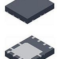
... Package Marking and Ordering Information Device Marking Device 22CA FDMS3604AS N7CC ©2011 Fairchild Semiconductor Corporation FDMS3604AS Rev.C4 General Description This device includes two specialized N-Channel MOSFETs in a dual PQFN package. The switch node has been internally = connected to enable easy placement and routing of synchronous ...
Page 2
... Fall Time f Q Total Gate Charge g Q Total Gate Charge g Q Gate to Source Gate Charge gs Q Gate to Drain “Miller” Charge gd ©2011 Fairchild Semiconductor Corporation FDMS3604AS Rev. °C unless otherwise noted J Test Conditions = 250 μ mA 250 μA, referenced to 25 °C I ...
Page 3
... Pulse Test: Pulse Width < 300 μs, Duty cycle < 2.0 N-ch device, the negative Vgs rating is for low duty cycle pulse ocurrence only. No continuous rating is implied based on starting 112 mJ is based on starting ©2011 Fairchild Semiconductor Corporation FDMS3604AS Rev. °C unless otherwise noted J Test Conditions 23A GS ...
Page 4
... PULSE DURATION = 80 s DUTY CYCLE = 0.5% MAX 150 1.5 2.0 2 GATE TO SOURCE VOLTAGE (V) GS Figure 5. Transfer Characteristics ©2011 Fairchild Semiconductor Corporation FDMS3604AS Rev. °C unless otherwise noted μ PULSE DURATION = 80 s DUTY CYCLE = 0.5% MAX 0.6 0.8 1 100 125 150 - 0.001 3.0 3 ...
Page 5
... Switching Capability 100 10 1 THIS AREA IS LIMITED SINGLE PULSE 0 MAX RATED 125 C/W θ 0.01 0.01 0 DRAIN to SOURCE VOLTAGE (V) DS Figure 11. Forward Bias Safe Operating Area ©2011 Fairchild Semiconductor Corporation FDMS3604AS Rev. °C unless otherwise noted 100 100 100us 100 ms 1s 10s DC ...
Page 6
... Typical Characteristics (Q1 N-Channel) 2 DUTY CYCLE-DESCENDING ORDER 0.5 0.2 0.1 0.05 0.1 0.02 0.01 0.01 0.001 - Figure 13. Junction-to-Ambient Transient Thermal Response Curve ©2011 Fairchild Semiconductor Corporation FDMS3604AS Rev. °C unless otherwise noted J SINGLE PULSE 125 C/W θ Note RECTANGULAR PULSE DURATION (sec) ...
Page 7
... 125 1.5 2.0 2 GATE TO SOURCE VOLTAGE (V) GS Figure 18. Transfer Characteristics ©2011 Fairchild Semiconductor Corporation FDMS3604AS Rev. unlenss otherwise noted J μ PULSE DURATION = 80 s DUTY CYCLE = 0.5% MAX 0.6 0.8 1.0 Figure 15. Normalized on-Resistance vs Drain 50 75 100 125 150 - 0.001 3.0 3.5 4 ...
Page 8
... THIS AREA IS 1 LIMITED SINGLE PULSE T = MAX RATED 0 120 C/W θ 0.01 0.01 0 DRAIN to SOURCE VOLTAGE (V) DS Figure 24. Forward Bias Safe Operating Area ©2011 Fairchild Semiconductor Corporation FDMS3604AS Rev. unless otherwise noted J 10000 160 120 100 100 1000 1000 100 ms 1s 10s DC ...
Page 9
... Typical Characteristics (Q2 N-Channel) 2 DUTY CYCLE-DESCENDING ORDER 0.5 0.2 0.1 0.05 0.1 0.02 0.01 0.01 0.001 - Figure 26. Junction-to-Ambient Transient Thermal Response Curve ©2011 Fairchild Semiconductor Corporation FDMS3604AS Rev. unless otherwise noted J SINGLE PULSE 120 C/W θ JA (Note 1d RECTANGULAR PULSE DURATION (sec NOTES: ...
Page 10
... FDMS3604AS 100 TIME (ns) Figure 27. FDMS3604AS SyncFET body diode reverse recovery characteristic ©2011 Fairchild Semiconductor Corporation FDMS3604AS Rev.C4 (continued) Schottky barrier diodes exhibit significant leakage at high tem- perature and high reverse voltage. This will increase the power in the device. 10 μ didt = 300 A/ s ...
Page 11
... As shown in the figure 29, the Power Stage solution rings significantly less than competitor solutions under the same set of test conditions. Power Stage Device Figure 29. Power Stage phase node rising edge, High Side Turn on *Patent Pending ©2011 Fairchild Semiconductor Corporation FDMS3604AS Rev.C4 Competitors solution 11 www.fairchildsemi.com ...
Page 12
... Power Stage is a high power density solution and all high current flow paths, such as VIN (D1), PHASE (S1/D2) and GND (S2), should be short and wide for better and stable current flow, heat radiation and system performance. A recommended layout proce- dure is discussed below to maximize the electrical and thermal performance of the part. ©2011 Fairchild Semiconductor Corporation FDMS3604AS Rev.C4 Figure 31. Recommended PCB Layout 12 www.fairchildsemi.com ...
Page 13
... Vias should be relatively large, around 8 mils to 10 mils, and of reasonable inductance. Critical high frequency components such as ceramic bypass caps should be located close to the part and on the same side of the PCB. If not feasible, they should be connected from the backside via a network of low inductance vias. ©2011 Fairchild Semiconductor Corporation FDMS3604AS Rev.C4 13 www.fairchildsemi.com ...
Page 14
... Dimensional Outline and Pad Layout ©2011 Fairchild Semiconductor Corporation FDMS3604AS Rev.C4 14 www.fairchildsemi.com ...
Page 15
... Definition of Terms Datasheet Identification Product Status Advance Information Formative / In Design Preliminary First Production No Identification Needed Full Production Obsolete Not In Production ©2011 Fairchild Semiconductor Corporation FDMS3604AS Rev.C4 ® * PDP SPM™ Power-SPM™ ® PowerTrench PowerXS™ SM Programmable Active Droop™ ® QFET QS™ ...