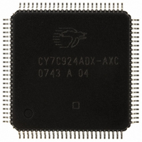
CY7C924ADX-AXC Cypress Semiconductor Corp, CY7C924ADX-AXC Datasheet - Page 6

CY7C924ADX-AXC
Manufacturer Part Number
CY7C924ADX-AXC
Description
IC TXRX HOTLINK 100LQFP
Manufacturer
Cypress Semiconductor Corp
Series
HOTlink™r
Type
Transceiverr
Specifications of CY7C924ADX-AXC
Package / Case
100-LQFP
Protocol
Fibre Channel
Voltage - Supply
4.5 V ~ 5.5 V
Mounting Type
Surface Mount
Product
Framer
Number Of Transceivers
1
Data Rate
622 Mbps
Supply Voltage (max)
5.5 V
Supply Voltage (min)
4.5 V
Supply Current (max)
250 mA
Maximum Operating Temperature
+ 70 C
Minimum Operating Temperature
0 C
Mounting Style
SMD/SMT
Operating Supply Voltage (typ)
5V
Screening Level
Commercial
Pin Count
100
Mounting
Surface Mount
Package Type
TQFP
Operating Supply Voltage (min)
4.5V
Operating Supply Voltage (max)
5.5V
Operating Temperature (min)
0C
Operating Temperature (max)
70C
Ic Interface Type
Parallel, Serial
Supply Voltage Range
4.5V To 5.5V
Operating Temperature Range
0°C To +70°C
Digital Ic Case Style
TQFP
No. Of Pins
100
No. Of Receivers
2
Frequency Max
50MHz
Rohs Compliant
Yes
Termination Type
SMD
Filter Terminals
SMD
Driver Case Style
TQFP
Lead Free Status / RoHS Status
Lead free / RoHS Compliant
Number Of Drivers/receivers
-
Lead Free Status / Rohs Status
Compliant
Other names
428-2918
CY7C924ADX-AXC
CY7C924ADX-AXC
Available stocks
Company
Part Number
Manufacturer
Quantity
Price
Company:
Part Number:
CY7C924ADX-AXC
Manufacturer:
CY
Quantity:
6
Company:
Part Number:
CY7C924ADX-AXC
Manufacturer:
CYPRESS
Quantity:
455
Company:
Part Number:
CY7C924ADX-AXC
Manufacturer:
Cypress Semiconductor Corp
Quantity:
10 000
Pin Descriptions
CY7C924ADX HOTLink Transceiver
Document #: 38-02008 Rev. *G
20
18
9
68
72
Number
Pin
TXSC/D*
TXEN*
TXSTOP*
TXCLK
TXFULL*
Name
(continued)
TTL input, sampled
on TXCLK↑ or
REFCLK↑,
Internal Pull Up
TTL input, sampled
on TXCLK↑ or
REFCLK↑,
Internal Pull Up
TTL input, sampled
on TXCLK↑,
Internal Pull Up
TTL clock input,
Internal Pull Up
3-state TTL output,
changes following
TXCLK↑ or
REFCLK↑
I/O Characteristics
Transmit Special Character or Data Select Input. When the Transmit FIFO is
enabled and the encoder is enabled (FIFOBYP* and ENCBYP* are HIGH), this
input is interpreted along with TXSVS and TXSOC (see
details).
When the Transmit FIFO is bypassed and encoding is enabled (FIFOBYP* is LOW
and ENCBYP* is HIGH), this signal controls whether the TXDATA[7:0] is sent as a
data or control character.
When the encoder is bypassed (ENCBYP* is LOW) TXSC/D* is ignored.
Transmit Enable Input. Data enable for the TXDATA[11:0] data bus write opera-
tions. Active HIGH when configured for Cascade timing (EXTFIFO is HIGH), active
LOW when configured for UTOPIA timing (EXTFIFO is LOW).
When the Transmit FIFO is enabled (FIFOBYP* is HIGH) and TXEN* is asserted,
data loads into the FIFO on every rising edge of TXCLK. When TXEN* is
deasserted with TXHALT* and TXSTOP* deasserted, data continues to read out
of the Transmit FIFO and is sent serially until the FIFO empties. At this time, C5.0
(K28.5) idle characters are transmitted.
When the Transmit FIFO is bypassed (FIFOBYP* is LOW) and TXEN* is asserted,
the parallel data on the TXDATA bus is clocked in and transmitted on every appro-
priate REFCLK rising edge. When TXEN* is deasserted, the parallel data bus is
ignored and C5.0 sync characters are transmitted instead.
Transmit Stop on Start_Of_Cell Input. While the Transmit FIFO and encoder are
enabled (FIFOBYP* and ENCBYP* are HIGH), this signal is used to prevent
queued data characters from being serially transmitted. While TXSTOP* is
deasserted, data flows through the Transmit FIFO without interruption. When
TXSTOP* is asserted, data transfers continue until a TXSOC bit is detected in the
character stream, at which point data transmission ceases. When transmission is
stopped, C5.0 (K28.5) characters are sent instead.
If data transmission is suspended due to a SOC character, pulsing TXSTOP*
deasserted then asserted will allow only the next cell (delimited by SOC bits) to be
transmitted.
When the Transmit FIFO is bypassed (FIFOBYP* = LOW) TXSTOP* has no
function.
When the Transmit FIFO is enabled (FIFOBYP* is HIGH) and the encoder is
bypassed (ENCBYP* is LOW), TXDATA[9]/TXHALT* is a data input and not
TXHALT*. In this mode, the TXSOC bit is not interpreted and the TXSTOP* input
assumes the same operation as TXHALT*. When TXSTOP* is asserted, data reads
from the Transmit FIFO are suspended and alternating disparity 10 bit equivalents
of C5.0 are transmitted instead.
Transmit FIFO Clock. The input clock for the parallel interface when the Transmit
FIFO is enabled (FIFOBYP* is HIGH). Samples all Transmit FIFO related interface
signals.
Transmit FIFO Full Status Flag. Active HIGH when configured for Cascade timing
(EXTFIFO is HIGH), active LOW when configured for UTOPIA timing (EXTFIFO is
LOW). The TXFULL* output is enabled when AM* is asserted, otherwise it is
High-Z.
When the Transmit FIFO is enabled (FIFOBYP* is HIGH), TXFULL* indicates a
Transmit FIFO full condition. When TXFULL* is first asserted, the Transmit FIFO
accepts up to eight additional write cycles without data loss.
When the Transmit FIFO is bypassed (FIFOBYP* is LOW), with RANGESEL HIGH
or SPDSEL LOW, TXFULL* toggles at half the REFCLK rate to provide a character
rate indication.
Signal Description
Table 2
CY7C924ADX
on page 16 for
Page 6 of 62


