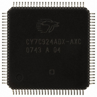
CY7C924ADX-AXC Cypress Semiconductor Corp, CY7C924ADX-AXC Datasheet - Page 11

CY7C924ADX-AXC
Manufacturer Part Number
CY7C924ADX-AXC
Description
IC TXRX HOTLINK 100LQFP
Manufacturer
Cypress Semiconductor Corp
Series
HOTlink™r
Type
Transceiverr
Specifications of CY7C924ADX-AXC
Package / Case
100-LQFP
Protocol
Fibre Channel
Voltage - Supply
4.5 V ~ 5.5 V
Mounting Type
Surface Mount
Product
Framer
Number Of Transceivers
1
Data Rate
622 Mbps
Supply Voltage (max)
5.5 V
Supply Voltage (min)
4.5 V
Supply Current (max)
250 mA
Maximum Operating Temperature
+ 70 C
Minimum Operating Temperature
0 C
Mounting Style
SMD/SMT
Operating Supply Voltage (typ)
5V
Screening Level
Commercial
Pin Count
100
Mounting
Surface Mount
Package Type
TQFP
Operating Supply Voltage (min)
4.5V
Operating Supply Voltage (max)
5.5V
Operating Temperature (min)
0C
Operating Temperature (max)
70C
Ic Interface Type
Parallel, Serial
Supply Voltage Range
4.5V To 5.5V
Operating Temperature Range
0°C To +70°C
Digital Ic Case Style
TQFP
No. Of Pins
100
No. Of Receivers
2
Frequency Max
50MHz
Rohs Compliant
Yes
Termination Type
SMD
Filter Terminals
SMD
Driver Case Style
TQFP
Lead Free Status / RoHS Status
Lead free / RoHS Compliant
Number Of Drivers/receivers
-
Lead Free Status / Rohs Status
Compliant
Other names
428-2918
CY7C924ADX-AXC
CY7C924ADX-AXC
Available stocks
Company
Part Number
Manufacturer
Quantity
Price
Company:
Part Number:
CY7C924ADX-AXC
Manufacturer:
CY
Quantity:
6
Company:
Part Number:
CY7C924ADX-AXC
Manufacturer:
CYPRESS
Quantity:
455
Company:
Part Number:
CY7C924ADX-AXC
Manufacturer:
Cypress Semiconductor Corp
Quantity:
10 000
Pin Descriptions
CY7C924ADX HOTLink Transceiver
Document #: 38-02008 Rev. *G
75
74
49
28
27
24, 25
Number
Pin
SPDSEL
RANGESEL
EXTFIFO
FIFOBYP*
ENCBYP*
RXMODE[1:0]
Name
(continued)
Static control input
TTL levels Normally
wired HIGH or LOW
Static control input
TTL levels Normally
wired HIGH or LOW
Static control input
TTL levels Normally
wired HIGH or LOW
Static control input
TTL levels Normally
wired HIGH or LOW
Static control input
TTL levels Normally
wired HIGH or LOW
Static control input
TTL levels Normally
wired HIGH or LOW
I/O Characteristics
Speed Select. Selects one of two operating data rate ranges for the device. When
the operating symbol rate is between 100 and 200 MBaud, SPDSEL must be HIGH.
When the operating symbol rate is between 50 and 100 MBaud, SPDSEL must be
LOW (see
Range Select. Selects the proper prescaler for the REFCLK input. See
the various relationships among REFCLK, SPDSEL, RANGESEL, FIFOBYP*,
ENCBYP* and BYTE8/10*.
When the Transmit FIFO is bypassed (FIFOBYP* is LOW) and REFCLK is a
nonunity multiple of the character rate (RANGESEL HIGH or SPDSEL LOW),
TXFULL* toggles at half the REFCLK rate to provide a character rate indication,
and to show when data can be accepted.
External FIFO Select. EXTFIFO indicates whether the device is used with external
FIFOs. It modifies the active level of the RXEN* and TXEN* inputs and the timing
of the Transmitter data bus according to the interface selected. When in UTOPIA
mode and not configured for external FIFOs (EXTFIFO is LOW), TXEN*, RXEN*
and all FIFO flags are active LOW. In this mode the active data transition for the
transmit data bus is within the same clock as the transmit interface is selected by
TXEN*.
When configured for Cascade mode where the CY7C924ADX device is cascaded
with external FIFOs (EXTFIFO is HIGH), TXEN, RXEN, the Full and Empty FIFO
flags are active HIGH (the Half-full flag is always active LOW). TXEN is driven by
the empty flag of an attached CY7C42X5 FIFO, and RXEN is driven by the Almost
Full flag of an attached CY7C42X5 FIFO. In this mode the active data transition for
the transmit data bus is in the clock cycle following the clock edge where transmit
interface is selected by TXEN*.
FIFO Bypass Select. When LOW, the Transmit and Receive FIFOs are bypassed.
In this mode TXCLK is not used. Instead all transmit data must be synchronous to
REFCLK. Transmit FIFO status flags are synchronized to REFCLK. RXCLK
becomes an output at the Receive PLL recovered character clock rate. All received
data and FIFO status flags are synchronized to RXCLK.
When HIGH, the Transmit and Receive FIFOs are enabled. In this mode all
Transmit FIFO writes are synchronized to TXCLK, and all Receive FIFO reads are
synchronous to the RXCLK input.
Encoder Bypass Select. When LOW, both the encoder and decoder are
bypassed. Data transmits in NRZ format, without encoding, LSB first. Received
data are presented to the interface as parallel characters without decoding.
When HIGH, data passes through both the 8B/10B encoder in the Transmit path
and the decoder in the Receive path.
Receive Discard Policy Select. These inputs select among the four data handling
and fill-character discard modes in the receiver. See
Table 5
on page 20).
Signal Description
Table 7
CY7C924ADX
on page 24.
Page 11 of 62
Table 5
for


