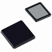
AD9911BCPZ Analog Devices Inc, AD9911BCPZ Datasheet - Page 9

AD9911BCPZ
Manufacturer Part Number
AD9911BCPZ
Description
IC DDS 500MSPS DAC 10BIT 56LFCSP
Manufacturer
Analog Devices Inc
Datasheet
1.AD9911BCPZ-REEL7.pdf
(44 pages)
Specifications of AD9911BCPZ
Resolution (bits)
10 b
Master Fclk
500MHz
Tuning Word Width (bits)
32 b
Voltage - Supply
1.71 V ~ 1.96 V
Operating Temperature
-40°C ~ 85°C
Mounting Type
Surface Mount
Package / Case
56-LFCSP
Transmitting Current
73mA
Data Rate
800Mbps
Rf Ic Case Style
LFCSP
No. Of Pins
56
Supply Voltage Range
1.71V To 1.89V, 3.135V To 3.465V
Operating Temperature Range
-40°C To +85°C
Msl
MSL 3 - 168 Hours
Lead Free Status / RoHS Status
Lead free / RoHS Compliant
For Use With
AD9911/PCBZ - BOARD EVAL FOR AD9911AD9911/PCB - BOARD EVAL FOR AD9911
Lead Free Status / Rohs Status
Compliant
Available stocks
Company
Part Number
Manufacturer
Quantity
Price
Company:
Part Number:
AD9911BCPZ
Manufacturer:
NXP
Quantity:
173
Part Number:
AD9911BCPZ
Manufacturer:
ADI/亚德诺
Quantity:
20 000
ABSOLUTE MAXIMUM RATINGS
Table 2.
Parameter
Maximum Junction Temperature
DVDD_I/O (Pin 49)
AVDD, DVDD
Digital Input Voltage (DVDD_I/O = 3.3 V)
Digital Output Current
Storage Temperature
Operating Temperature
Lead Temperature (10 sec Soldering)
ESD CAUTION
ESD (electrostatic discharge) sensitive device. Electrostatic charges as high as 4000 V readily accumulate on
the human body and test equipment and can discharge without detection. Although this product features
proprietary ESD protection circuitry, permanent damage may occur on devices subjected to high energy
electrostatic discharges. Therefore, proper ESD precautions are recommended to avoid performance
degradation or loss of functionality.
EQUIVALENT INPUT AND OUTPUT CIRCUITS
θ
θ
JA
JC
INPUT
NOTES
1. AVOID OVERDRIVING DIGITAL
INPUTS.
Figure 3. CMOS Digital Inputs
DVDD_I/O = 3.3V
DIGITAL INPUTS
CMOS
OUTPUT
Rating
150°C
4 V
2 V
−0.7 V to +4 V
5 mA
–65°C to +150°C
–40°C to +85°C
300°C
21°C/W
2°C/W
NOTES
1. TERMINATE OUTPUTS
2. DO NOT EXCEED
IOUT
DAC OUTPUTS
INTO AVDD.
OUTPUTS VOLTAGE
COMPLIANCE.
Figure 4. DAC Outputs
Rev. 0 | Page 9 of 44
IOUT
Stresses above those listed under Absolute Maximum Ratings
may cause permanent damage to the device. This is a stress
rating only; functional operation of the device at these or any
other conditions above those indicated in the operational
section of this specification is not implied. Exposure to absolute
maximum rating conditions for extended periods may affect
device reliability.
NOTES
1. REF_CLK INPUTS ARE INTERNALLY BIASED AND
2. OSC INPUTS ARE DC-COUPLED.
AVDD
NEED TO BE AC-COUPLED.
REF_CLK
1.5kΩ
Figure 5. REF_CLK Inputs
REF_CLK INPUTS
Z
AMP
AVDD
Z
1.5kΩ
REF_CLK
AD9911
OSC
AVDD


