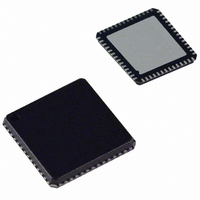
AD9911BCPZ Analog Devices Inc, AD9911BCPZ Datasheet - Page 25

AD9911BCPZ
Manufacturer Part Number
AD9911BCPZ
Description
IC DDS 500MSPS DAC 10BIT 56LFCSP
Manufacturer
Analog Devices Inc
Datasheet
1.AD9911BCPZ-REEL7.pdf
(44 pages)
Specifications of AD9911BCPZ
Resolution (bits)
10 b
Master Fclk
500MHz
Tuning Word Width (bits)
32 b
Voltage - Supply
1.71 V ~ 1.96 V
Operating Temperature
-40°C ~ 85°C
Mounting Type
Surface Mount
Package / Case
56-LFCSP
Transmitting Current
73mA
Data Rate
800Mbps
Rf Ic Case Style
LFCSP
No. Of Pins
56
Supply Voltage Range
1.71V To 1.89V, 3.135V To 3.465V
Operating Temperature Range
-40°C To +85°C
Msl
MSL 3 - 168 Hours
Lead Free Status / RoHS Status
Lead free / RoHS Compliant
For Use With
AD9911/PCBZ - BOARD EVAL FOR AD9911AD9911/PCB - BOARD EVAL FOR AD9911
Lead Free Status / Rohs Status
Compliant
Available stocks
Company
Part Number
Manufacturer
Quantity
Price
Company:
Part Number:
AD9911BCPZ
Manufacturer:
NXP
Quantity:
173
Part Number:
AD9911BCPZ
Manufacturer:
ADI/亚德诺
Quantity:
20 000
sweep is then complete and the output held constant in
frequency. See Figure 43 for the linear sweep circuitry.
Figure 45 depicts a frequency sweep with no-dwell mode
disabled. In this mode, the output follows the state of the profile
pin. A phase or amplitude sweep works in the same manner
with fewer bits.
LINEAR SWEEP NO DWELL MODE
To enable linear sweep no dwell mode, set CFR <15>. The rising
sweep is started by setting the profile input pin to 1. The
frequency, phase or amplitude continues to sweep up at the rate
set by the rising sweep ramp rate and the resolution set by the
LOAD CONTROL
RDW
FDW
RATE TIME
LOGIC
PROFILE PIN
FTW1
FTW0
MUX
0
1
f
OUT
SINGLE–TONE
8-BIT LOADABLE DOWN COUNTER
MODE
N
PS<1> = 0
0
RAMP RATE TIMER:
FSRR
0
MUX
MUX
0
1
RSRR
8
1
N
A
Figure 44. Linear Sweep Mode Enabled—No Dwell Bit Set
PS<1> = 1 PS<1> = 0
PROFILE PIN
Figure 43. Linear Sweep Block Circuitry
N
ACCUMULATOR RESET
B
Rev. 0 | Page 25 of 44
A
PS<1> = 1
LOGIC
SWEEP ACCUMULATOR
Z
–1
rising delta tuning word, until it reaches E0. The output then
reverts to the S0 and stalls until high is detected on the
profile pin.
Figure 44 demonstrates the no-dwell mode. The points labeled
A indicate where a rising edge is detected on the profile pin.
Points labeled B indicate at which points where the AD9911 has
determined that the output has reached E0 and reverts to S0.
The falling ramp rate register and the falling delta word are
unused in this mode.
N
B
0
PS<1> = 0
KEEP SWEEP BETWEEN
MUX
0
1
LIMIT LOGIC TO
S0 AND E0
A
MUX
0
1
PS<1> = 1
SWEEP ADDER
B
N
CTW1
N
CTW0
TIME
N
AD9911


