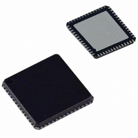
AD9911BCPZ Analog Devices Inc, AD9911BCPZ Datasheet - Page 31

AD9911BCPZ
Manufacturer Part Number
AD9911BCPZ
Description
IC DDS 500MSPS DAC 10BIT 56LFCSP
Manufacturer
Analog Devices Inc
Datasheet
1.AD9911BCPZ-REEL7.pdf
(44 pages)
Specifications of AD9911BCPZ
Resolution (bits)
10 b
Master Fclk
500MHz
Tuning Word Width (bits)
32 b
Voltage - Supply
1.71 V ~ 1.96 V
Operating Temperature
-40°C ~ 85°C
Mounting Type
Surface Mount
Package / Case
56-LFCSP
Transmitting Current
73mA
Data Rate
800Mbps
Rf Ic Case Style
LFCSP
No. Of Pins
56
Supply Voltage Range
1.71V To 1.89V, 3.135V To 3.465V
Operating Temperature Range
-40°C To +85°C
Msl
MSL 3 - 168 Hours
Lead Free Status / RoHS Status
Lead free / RoHS Compliant
For Use With
AD9911/PCBZ - BOARD EVAL FOR AD9911AD9911/PCB - BOARD EVAL FOR AD9911
Lead Free Status / Rohs Status
Compliant
Available stocks
Company
Part Number
Manufacturer
Quantity
Price
Company:
Part Number:
AD9911BCPZ
Manufacturer:
NXP
Quantity:
173
Part Number:
AD9911BCPZ
Manufacturer:
ADI/亚德诺
Quantity:
20 000
Bit 7 of the instruction byte (R/Wb) determines whether a read
or write data transfer occurs after the instruction byte write. set
indicates a read operation; Cleared indicates a write operation.
Bit 4 to Bit 0 of the instruction byte determine which register is
accessed during the data transfer portion of the
communications cycle. The internal byte addresses are
generated by the AD9911.
I/O PORT PIN DESCRIPTION
Data Clock (SCLK)
The clock pin is used to synchronize data to and from the
internal state machines of the AD9911.
Chip Select ( CS )
The chip select pin allows more than one AD9911 device to be
on the same communications lines. The chip select is an active
low enable pin. Defined SDIO inputs go to a high impedance
state when CS is high. If CS is driven high during any
communications cycle, that cycle is suspended until CS is
reactivated low.
Data I/O (SDIO_0:3)
Of the four SDIO pins, only the SDIO_0 pin is dedicated to this
function. SDIO_1:3 can be used to control the ramping of the
output amplitude. Bits <2:1> in the channel select register (CSR
Register 0x00) control the configuration of these pins. See the
I/O Modes of Operation section for more information.
I/O PORT FUNCTION DESCRIPTION
Serial Data Out (SDO)
The SDO function is available in single-bit (3-wire) mode only.
In SDO mode, data is read from the SDIO_2 pin for protocols
that use separate lines for reading and writing data (see Table 23
for pin configuration options). Bits <2:1> in the CSR register
(Register 0x00) control the configuration of this pin. The SDO
function is not available in 2-bit and 4-bit I/O modes.
SYNC_I/O
The SYNC_I/O function is available in 1-bit and 2-bit modes.
SDIO_3 serves as the SYNC_I/O pin, as configured by Bits
<2:1> in the CSR register (Register 0x00). Otherwise, the
SYNC_I/O function is used to synchronize the I/O port state
machines without affecting the addressable register contents.
An active high input on the SYNC_I/O pin causes the current
communication cycle to abort. After SDIO_3 returns low (Logic
0), another communication cycle can begin. The SYNC_I/O
function is not available in 4-bit I/O mode.
MSB/LSB TRANSFER DESCRIPTION
The AD9911 I/O port supports either MSB or LSB first data
formats. This functionality is controlled by CSR <0> in the
channel select register (CSR). MSB-first is the default. When
CSR <0> is set, the I/O port is LSB-first. The instruction byte
must be written in the manner selected by CSR <0>.
Rev. 0 | Page 31 of 44
Example
To write the Function Register 1 (FR1) in MSB-first format,
apply an instruction byte of MSB > 00000001 < LSB, starting
with the MSB. The internal controller recognizes a write
transfer of three bytes starting with the MSB, Bit <23>, in the
FR1 address (Register 0x01). Bytes are written on each
consecutive rising SCLK edge until Bit<0> is transferred. This
indicates the I/O communication cycle is complete and the next
byte is considered an instruction byte.
To write the Function Register 1 (FR1) in LSB-first format,
apply an instruction byte of MSB > 00000001 < LSB, starting
with the LSB. The internal controller recognizes a write transfer
of three bytes, starting with the LSB, Bit <0>, in the FR1 address
(Register 0x01). Bytes are written on each consecutive rising
SCLK edge until Bit <23> is transferred. Once the last data bit is
written, the I/O communication cycle is complete and the next
byte is considered an instruction byte.
I/O MODES OF OPERATION
There are four selectable modes of I/O port operation:
•
•
•
•
Table 23 displays the function of all six I/O interface pins,
depending on the mode of I/O operation selected.
Table 23. I/O Port Pin Function vs. I/O Mode
Pin
Name
SCLK
CSB
SDIO_0
SDIO_1
SDIO_2
SDIO_3
1
The two bits, CSR <2:1>, in the channel select register set the
I/O mode of operation. These bits are defined as follows:
CSR <2:1> = 00. Single bit serial mode (2-wire mode)
CSR <2:1> = 01. Single bit serial mode (3-wire mode)
CSR <2:1> = 10. 2-bit mode
CSR <2:1> = 11. 4-bit mode
In this mode, these pins can be used for RU/RD operation
Single-bit serial 2-wire mode (default mode).
Single-bit, 3-wire mode.
2-bit mode.
4-bit mode (SYNC_I/O not available).
Single Bit,
2-Wire
Mode
I/O
Clock
Chip
Select
Data I/O
Not used
for SDIO
Not used
for SDIO
SYNC_I/O
1
1
Single Bit,
3-Wire
Mode
I/O
Clock
Chip
Select
Data In
Not used
for SDIO
Serial Data
Out (SDO)
SYNC_I/O
1
2-Bit Mode 4-Bit Mode
I/O
Clock
Chip
Select
Data I/O
Data I/O
Not used
for SDIO
SYNC_I/O
1
.
I/O
Clock
Chip Select
Data I/O
Serial Data
I/O
Serial Data
I/O
Data I/O
AD9911


