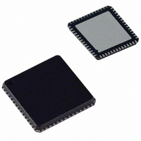
AD9911BCPZ Analog Devices Inc, AD9911BCPZ Datasheet - Page 22

AD9911BCPZ
Manufacturer Part Number
AD9911BCPZ
Description
IC DDS 500MSPS DAC 10BIT 56LFCSP
Manufacturer
Analog Devices Inc
Datasheet
1.AD9911BCPZ-REEL7.pdf
(44 pages)
Specifications of AD9911BCPZ
Resolution (bits)
10 b
Master Fclk
500MHz
Tuning Word Width (bits)
32 b
Voltage - Supply
1.71 V ~ 1.96 V
Operating Temperature
-40°C ~ 85°C
Mounting Type
Surface Mount
Package / Case
56-LFCSP
Transmitting Current
73mA
Data Rate
800Mbps
Rf Ic Case Style
LFCSP
No. Of Pins
56
Supply Voltage Range
1.71V To 1.89V, 3.135V To 3.465V
Operating Temperature Range
-40°C To +85°C
Msl
MSL 3 - 168 Hours
Lead Free Status / RoHS Status
Lead free / RoHS Compliant
For Use With
AD9911/PCBZ - BOARD EVAL FOR AD9911AD9911/PCB - BOARD EVAL FOR AD9911
Lead Free Status / Rohs Status
Compliant
Available stocks
Company
Part Number
Manufacturer
Quantity
Price
Company:
Part Number:
AD9911BCPZ
Manufacturer:
NXP
Quantity:
173
Part Number:
AD9911BCPZ
Manufacturer:
ADI/亚德诺
Quantity:
20 000
AD9911
modulating phase or amplitude, the word value must be MSB-
aligned in the profile registers; excess bits are ignored. In
modulation mode, bits CFR <23:22> and FR1 <9:8> configure
the modulation type and level. See Table 6 and Table 7 for
settings. Note that the linear sweep enable bit must be set to
Logic 0 in modulation mode.
Table 6.
CFR <23:22>
0
0
1
1
Table 7.
FR1 <9:8>
0
0
1
1
When both modulation and the RU/RD feature are desired,
unused profile pins or SDIO pins can be assigned. SDIO pins
can only be used for RU/RD.
Table 8.
RU/RD Bits
FR1 <11:10>
0
0
1
1
If profile pins are used for RU/RD, Logic 0 sets for ramp up and
Logic 1 sets for ramp down.
To support RU/RD flexibility, it is necessary to assign the profile
pins and/or SDIO Pin 1 to Pin 3 to CH1 operation. This is
controlled by the profile pin configuration (PPC) or PPC bits
(FR1 <14:12>). The modulation descriptions that follow include
data pin assignment. In the modulation descriptions, an “x”
indicates that it does not matter.
2-Level Modulation—No RU/RD
Modulation level bits are set to 00 (2-level). AFP bits are set to
the desired modulation. RU/RD bits and the linear sweep bit are
disabled. Table 9 displays how the profile pins are assigned.
Table 9. 2-Level Modulation — No RU/RD
Bits FR1<14:12>
x
0
1
0
1
x
0
1
0
1
0
1
0
1
Description
RU/RD disabled.
Profile Pin 2 and Pin 3 configured for RU/RD
operation.
Profile Pin 3 configured for RU/RD operation.
SDIO Pin 1, Pin 2, and Pin 3 configured for
RU/RD operation. Forces the I/O to be used only
in 1-bit mode.
x
CFR <14>
x
0
0
0
Description
2-level modulation
4-level modulation
8-level modulation
16-level modulation
P0
N/A
Description
Modulation disabled
Amplitude modulation
Frequency modulation
Phase modulation
P1
CH1
P2
N/A
P3
N/A
Rev. 0 | Page 22 of 44
As shown in Table 9, only Profile Pin P1 can be used to
modulate CH1. If Pin P1 is Logic 0 and FSK modulation is
desired, then Profile Register 0 (Register 0x04) frequency is
chosen. If Pin P1 is Logic 1, then Profile Register 1
(Register 0x0A) frequency is chosen.
4-Level Modulation—No RU/RD
Modulation level bits are set to 01 (4-level). AFP bits are set to
the desired modulation. RU/RD bits and the linear sweep bit are
disabled. Table 10 displays how the profile pins are assigned.
Table 10. 4-Level Modulation—No RU/RD
Profile Pin Configuration (PPC) Bits
FR1 <14:12>
0
For this condition, the profile register chosen is based on the
2 bit value presented to profile pins <P0:P1>. For example, if
PPC = 011 and <P0:P1>= 11, then the contents of Profile
Register 3 (Register 0x0C) are presented to CH1 output.
8-Level Modulation—No RU/RD
Modulation level bits are set to 10 (8-level). AFP bits are set to
the desired modulation. RU/RD bits and the linear sweep bit are
disabled. Table 11 shows the assignment of profile pins and
channels.
Table 11. 8-Level Modulation—No RU/RD
Profile Pin Config. Bits
FR1 <14:12>
x
For this condition, the profile register (1 of 8) chosen is based
on the 3-bit value presented to the Profile Pin P0 to Pin P2. For
example, if PPC = x01 and <P0:P2> = 111, then the contents of
Profile Register 7 (Register 0x10) are presented to CH1 output.
16-Level Modulation—No RU/RD
Modulation level bits are set to 11 (16-level). AFP bits are set to
the desired modulation. RU/RD bits and the linear sweep bit are
disabled. Table 12 displays how the profile pins and channels are
assigned.
Table 12. 16-Level Modulation—No RU/RD
Profile Pin Config. (PPC) Bits
FR1 <14:12>
x
For these conditions, the profile register chosen is based on the
4-bit value presented to Profile Pin P0 to Pin P3. For example, if
PPC = x01 and <P0:P3>= 1110, then the contents of Profile
Register 14 (Register 0x17) are presented to CH1 output.
2-Level Modulation Using Profile Pins for RU/RD
When the RU/RD bits = 01, either Profile Pin P2 or Pin P3 are
available for RU/RD. Note that only a modulation level of two is
available when RU/RD bits = 01. See Table 13 for available pin
assignments.
0
0
1
1
1
1
P0
CH1
P0
CH1
P0
CH1
P1
CH1
P1
CH1
P1
CH1
P2
CH1
P2
CH1
P2
N/A
P3
CH1
P3
x
P3
N/A


