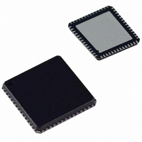
AD9911BCPZ Analog Devices Inc, AD9911BCPZ Datasheet - Page 32

AD9911BCPZ
Manufacturer Part Number
AD9911BCPZ
Description
IC DDS 500MSPS DAC 10BIT 56LFCSP
Manufacturer
Analog Devices Inc
Datasheet
1.AD9911BCPZ-REEL7.pdf
(44 pages)
Specifications of AD9911BCPZ
Resolution (bits)
10 b
Master Fclk
500MHz
Tuning Word Width (bits)
32 b
Voltage - Supply
1.71 V ~ 1.96 V
Operating Temperature
-40°C ~ 85°C
Mounting Type
Surface Mount
Package / Case
56-LFCSP
Transmitting Current
73mA
Data Rate
800Mbps
Rf Ic Case Style
LFCSP
No. Of Pins
56
Supply Voltage Range
1.71V To 1.89V, 3.135V To 3.465V
Operating Temperature Range
-40°C To +85°C
Msl
MSL 3 - 168 Hours
Lead Free Status / RoHS Status
Lead free / RoHS Compliant
For Use With
AD9911/PCBZ - BOARD EVAL FOR AD9911AD9911/PCB - BOARD EVAL FOR AD9911
Lead Free Status / Rohs Status
Compliant
Available stocks
Company
Part Number
Manufacturer
Quantity
Price
Company:
Part Number:
AD9911BCPZ
Manufacturer:
NXP
Quantity:
173
Part Number:
AD9911BCPZ
Manufacturer:
ADI/亚德诺
Quantity:
20 000
AD9911
Single-Bit Serial (2- and 3-Wire) Modes
The single-bit serial mode interface allows read/write access to
all registers that configure the AD9911. MSB-first or LSB-first
transfer formats and the SYNC_I/O function are supported.
In 2-wire mode, the SDIO_0 pin is the single serial data I/O pin.
In 3-wire mode, the SDIO_0 pin is the serial data input pin and
the SDIO_2 pin is the output. For both modes, the SDIO_3 pin
is configured as an input and operates as the SYNC_I/O pin.
The SDIO_1 pin is unused.
2-Bit Mode
The SPI port operation in 2-bit mode is identical to the SPI port
operation in single bit mode, except that two bits of data are
registered on each rising edge of SCLK, cutting in half the
number of cycles required to program the device. The SDIO_0
pin contains the even numbered data bits using the notation D
<7:0> while the SDIO_1 pin contains the odd numbered data
bits regardless of whether in MSB- or LSB-first format (see
Figure 47).
4-Bit Mode
The SPI port in 4-bit mode is identical to the SPI port in single
bit mode, except that four bits of data are registered on each
rising edge of SCLK.
SDIO_0
SCLK
CS
(I0)
I7
SDIO_1
SDIO_0
(I1)
I6
SCLK
CS
INSTRUCTION CYCLE
(I2)
I5
(I3)
I4
Figure 50. Single-Bit Serial Mode Write Timing—Clock Stall Low
INSTRUCTION CYCLE
(I1)
(I0)
I7
I6
Figure 51. 2-Bit Mode Write Timing—Clock Stall Low
(I4)
I3
(I3)
(I2)
I5
I4
(I5)
I2
(I5)
(I4)
I3
I2
(I6)
I1
Rev. 0 | Page 32 of 44
(I7)
(I6)
I1
I0
(I7)
I0
This reduces by 75% the number of cycles required to program
the device. Note that when reprogramming the device for 4-bit
mode, it is important to keep the SDIO_3 pin at Logic 0 until
the device is programmed out of the single bit serial mode.
Failure to do so can result in the I/O port controller being out of
sequence.
Figure 50 through Figure 52 are write timing diagrams for the
I/O modes available. Both MSB and LSB-first modes are shown.
LSB-first bits are shown in parenthesis. The clock stall low/high
feature shown is not required, but rather is used to show that
data (SDIO) must have the proper setup time relative to the
rising edge of SCLK.
Figure 53 through Figure 56 are read timing diagrams for each
I/O mode available. Both MSB and LSB-first modes are shown.
LSB-first bits are shown in parenthesis. The clock stall low/high
feature shown is not required. It is used to show that data
(SDIO) must have the proper set-up time relative to the rising
edge of SCLK for the instruction byte and the read data that
follows the falling edge of SCLK.
(D1)
(D0)
D7
D6
(D0)
D7
DATA TRANSFER CYCLE
(D3)
(D2)
D5
D4
(D1)
D6
(D5)
(D4)
D3
D2
(D2)
DATA TRANSFER CYCLE
D5
(D6)
(D7)
D1
D0
(D3)
D4
(D4)
D3
(D5)
D2
(D6)
D1
(D7)
D0


