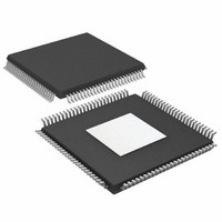
AD9858BSVZ Analog Devices Inc, AD9858BSVZ Datasheet - Page 28

AD9858BSVZ
Manufacturer Part Number
AD9858BSVZ
Description
IC DDS DAC 10BIT 1GSPS 100-TQFP
Manufacturer
Analog Devices Inc
Datasheet
1.AD9858BSVZ.pdf
(32 pages)
Specifications of AD9858BSVZ
Design Resources
Low Jitter Sampling Clock Generator for High Performance ADCs Using AD9958/9858 and AD9515 (CN0109)
Resolution (bits)
10 b
Master Fclk
1GHz
Tuning Word Width (bits)
32 b
Voltage - Supply
3.14 V ~ 3.47 V
Operating Temperature
-40°C ~ 85°C
Mounting Type
Surface Mount
Package / Case
100-TQFP Exposed Pad, 100-eTQFP, 100-HTQFP, 100-VQFP
Pll Type
Frequency Synthesis
Frequency
1GHz
Supply Voltage Range
3.135 To 3.165V, 4.75V To 5.25V
Digital Ic Case Style
TQFP
No. Of Pins
100
Operating Temperature Range
-40°C To +85°C
Lead Free Status / RoHS Status
Lead free / RoHS Compliant
For Use With
AD9858/TLPCBZ - BOARD EVAL TRANSLATION LOOP
Lead Free Status / RoHS Status
Lead free / RoHS Compliant, Lead free / RoHS Compliant
Available stocks
Company
Part Number
Manufacturer
Quantity
Price
Company:
Part Number:
AD9858BSVZ
Manufacturer:
ADI
Quantity:
98
Company:
Part Number:
AD9858BSVZ
Manufacturer:
Analog Devices Inc
Quantity:
10 000
Part Number:
AD9858BSVZ
Manufacturer:
ADI/亚德诺
Quantity:
20 000
AD9858
EVALUATION BOARDS
The AD9858 has three different evaluation board designs. The
first design is the traditional DDS evaluation board (see Figure 38).
In this design, the DDS is clocked and the output is taken
directly from the DAC. The analog mixer and PLL blocks are
made available for separate evaluation.
The second design is a fractional divide loop (see Figure 39).
This evaluation board was designed to incorporate the DDS, the
phase frequency detector, and the charge pump. In this
application, the DDS is used in a PLL loop. Unlike a fixed
divider used in traditional PLL loops, the output signal is
divided and fed back to the phase frequency detector by the
DDS. To do this, the output signal of the PLL loop is fed to the
DDS as REFCLK. The DDS is programmed to match the
reference input frequency. Because the DDS output frequency
can take on 2
the PLL loop output frequency, this enables frequency
resolution on the order of 470 MHz, assuming a PLL loop
output frequency of 2 GHz.
32
potential values between 0 Hz and one-half of
Rev. C | Page 28 of 32
The third design is a translation loop or offset loop (see Figure 37).
In this design, the analog mixer is incorporated into the feedback
path of the loop. This allows direct up-conversion to the
transmission frequency.
The three evaluation boards have separate schematics, BOMs, and
instructions. See
Table 13. Evaluation Boards for the AD9858
Model
AD9858/PCBZ
AD9858/FDPCB
AD9858/TLPCBZ
www.analog.com/dds
Description
AD9858 Frequency Synthesizer Board
AD9858 Fractional Divide Loop Frequency
Synthesizer Board
AD9858 Translation Loop Frequency
Synthesizer Board
for more information.


