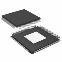
AD9858BSVZ Analog Devices Inc, AD9858BSVZ Datasheet - Page 24

AD9858BSVZ
Manufacturer Part Number
AD9858BSVZ
Description
IC DDS DAC 10BIT 1GSPS 100-TQFP
Manufacturer
Analog Devices Inc
Datasheet
1.AD9858BSVZ.pdf
(32 pages)
Specifications of AD9858BSVZ
Design Resources
Low Jitter Sampling Clock Generator for High Performance ADCs Using AD9958/9858 and AD9515 (CN0109)
Resolution (bits)
10 b
Master Fclk
1GHz
Tuning Word Width (bits)
32 b
Voltage - Supply
3.14 V ~ 3.47 V
Operating Temperature
-40°C ~ 85°C
Mounting Type
Surface Mount
Package / Case
100-TQFP Exposed Pad, 100-eTQFP, 100-HTQFP, 100-VQFP
Pll Type
Frequency Synthesis
Frequency
1GHz
Supply Voltage Range
3.135 To 3.165V, 4.75V To 5.25V
Digital Ic Case Style
TQFP
No. Of Pins
100
Operating Temperature Range
-40°C To +85°C
Lead Free Status / RoHS Status
Lead free / RoHS Compliant
For Use With
AD9858/TLPCBZ - BOARD EVAL TRANSLATION LOOP
Lead Free Status / RoHS Status
Lead free / RoHS Compliant, Lead free / RoHS Compliant
Available stocks
Company
Part Number
Manufacturer
Quantity
Price
Company:
Part Number:
AD9858BSVZ
Manufacturer:
ADI
Quantity:
98
Company:
Part Number:
AD9858BSVZ
Manufacturer:
Analog Devices Inc
Quantity:
10 000
Part Number:
AD9858BSVZ
Manufacturer:
ADI/亚德诺
Quantity:
20 000
AD9858
CFR[22]: Auto Clear Phase Accumulator Bit
When CFR[22] = 0 (default), a new frequency tuning word is
applied to the input of the phase accumulator and added to the
currently stored value.
When CFR[22] = 1, this bit automatically synchronously clears
(loads zeros into) the phase accumulator for one cycle upon
reception of the FUD sequence indicator.
CFR[21]: Load Delta Frequency Timer
When CFR[21] = 0 (default), the contents of the delta frequency
ramp rate word are loaded into the ramp rate timer (down counter)
upon detection of a FUD sequence.
When CFR[21] = 1, the contents of the delta frequency ramp
rate word are loaded into the ramp rate timer upon timeout
with no regard to the state of the FUD sequence indicator (that
is, the FUD sequence indicator is ignored).
CFR[20]: Clear Frequency Accumulator Bit
When CFR[20] = 1, the frequency accumulator is synchronously
cleared and is held clear until CFR[20] is returned to a Logic 0
state (default).
CFR[19]: Clear Phase Accumulator Bit
When CFR[19] = 1, the phase accumulator is synchronously
cleared and is held clear until CFR[19] is returned to a Logic 0
state (default).
CFR[18]: Not Used.
CFR[17]: Fast Lock Enable Bit
When CFR[17] = 0 (default), the PLL’s fast lock algorithm is
disabled. When CFR[17] = 1, the PLL’s fast-lock algorithm is active.
CFR[16]: FTW for Fast Lock Bit
This bit allows the user to control whether or not the PLL’s fast
lock algorithm uses the tuning word value to determine
whether or not to enter fast locking mode.
When CFR[16] = 0 (default), the fast locking algorithm of the
PLL considers the relationship between the programmed
frequency tuning word and the instantaneous frequency as part
of the locking process.
When CFR[16] = 1, the fast locking algorithm of the PLL does
not use the frequency tuning word as part of the locking process.
CFR[15]: Frequency Sweep Enable Bit
When CFR[15] = 0 (default), the device is in single-tone mode.
When CFR[15] = 1, the device is in the frequency sweep mode.
CFR[14]: Enable Sine Output Bit
When CFR[14] = 0 (default), the angle-to-amplitude conversion
logic employs a cosine function.
When CFR[14] = 1, the angle-to-amplitude conversion logic
employs a sine function.
Rev. C | Page 24 of 32
CFR[13]: Charge Pump Offset Bit
When CFR[13] = 0 (default), the charge pump operates with
normal current settings.
When CFR[13] = 1, the charge pump operates with offset
current settings (see Charge Pump section).
CFR[12:11]: Phase Detector Divider Ratio (N)
These bits set the phase detector divide value (see Table 10).
Table 10.
CFR[12:11]
00
01
1x
CFR[10]: Charge Pump Polarity Bit
When CFR[10] = 0 (default), the charge pump is set up for
operation with a ground-referenced VCO. In this mode, the charge
pump sources current when the frequency at PD
the frequency at DIV
When CFR[10] = 1, the charge pump is set up for a supply-
referenced VCO. In this mode, the source/sink operation of the
charge pump is opposite that for a ground-referenced VCO.
CFR[9:8]: Phase Detector Divider Ratio (M)
These bits set the phase detector divide value (see Table 11).
Table 11.
CFR[9:8]
00
01
1x
CFR[7]: Not Used
CFR[6]: 2 GHz Divider Disable Bit
When CFR[6] = 0 (default), the REFCLK divide-by-2 function
is enabled. REFCLK input can be up to 2 GHz.
When CFR[6] = 1, the REFCLK divide-by-2 function is
disabled. REFCLK input must be no more than 1 GHz.
CFR[5]: SYNCLK Disable Bit
When CFR[5] = 0 (default), the SYNCLK pin is active.
When CFR[5] = 1, the SYNCLK pin assumes a static Logic 0
state (disabled). In this state, the pin drive logic is shut down to
keep noise generated by the digital circuitry at a minimum.
However, the synchronization circuitry remains active (internally)
to maintain normal device timing.
Phase Detector Divider Ratio (M)
1
2
4
Phase Detector Divider Ratio (N)
1
2
4
IN
. It sinks current when the opposite is true.
IN
Notes
Default value
LSB ignored
Notes
Default value
LSB ignored
is less than


