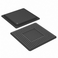
DS21FF44 Maxim Integrated Products, DS21FF44 Datasheet - Page 65

DS21FF44
Manufacturer Part Number
DS21FF44
Description
IC FRAMER E1 4X4 16CH 300-BGA
Manufacturer
Maxim Integrated Products
Datasheet
1.DS21FT44N.pdf
(117 pages)
Specifications of DS21FF44
Controller Type
E1 Framer
Interface
Parallel/Serial
Voltage - Supply
2.97 V ~ 3.63 V
Current - Supply
300mA
Operating Temperature
0°C ~ 70°C
Mounting Type
Surface Mount
Package / Case
300-BGA
Lead Free Status / RoHS Status
Contains lead / RoHS non-compliant
Available stocks
Company
Part Number
Manufacturer
Quantity
Price
DS21FT44/DS21FF44
17.1. Receive Side
If the receive side elastic store is enabled (RCR2.1=1), then the user must provide either a 1.544MHz
(RCR2.2 =0) or 2.048MHz (RCR2.2=1) clock at the RSYSCLK pin. The user has the option of either
providing a frame/multiframe sync at the RSYNC pin (RCR1.5=1) or having the RSYNC pin provide a
pulse on frame/multiframe boundaries (RCR1.5=0). If the user wishes to obtain pulses at the frame
boundary, then RCR1.6 must be set to zero and if the user wishes to have pulses occur at the multiframe
boundary, then RCR1.6 must be set to one. The DS21Q44 will always indicate frame boundaries by the
RFSYNC output whether the elastic store is enabled or not. If the elastic store is enabled, then either CAS
(RCR1.7=0) or CRC4 (RCR1.7=1) multiframe boundaries will be indicated by the RMSYNC output. If
the user selects to apply a 1.544MHz clock to the RSYSCLK pin, then every fourth channel of the
received E1 data is deleted and an F-bit position (which will be forced to one) is inserted. Hence,
Channels 1, 5, 9, 13, 17, 21, 25, and 29 (timeslots 0, 4, 8, 12, 16, 20, 24, and 28) will be deleted from the
received E1 data stream. Also, in 1.544MHz applications, the RCHBLK output will not be active in
Channels 25 through 32 (or in other words, RCBR4 is not active). See Section 22 for timing details. If the
512-bit elastic buffer either fills or empties, a controlled slip will occur. If the buffer empties, then a full
frame of data (256 bits) will be repeated at RSER and the SR1.4 and RIR.3 bits will be set to a one. If the
buffer fills, then a full frame of data will be deleted and the SR1.4 and RIR.4 bits will be set to a one.
17.2. Transmit Side
The operation of the transmit elastic store is very similar to the receive side. The transmit side elastic
store is enabled by CCR3.7. A 1.544MHz (CCR3.1=0) or 2.048MHz (CCR3.1=1) clock can be applied to
the TSYSCLK input. The TSYSCLK can be a bursty clock with rates up to 8.192MHz. If the user selects
to apply a 1.544MHz clock to the TSYSCLK pin, then the data sampled at TSER will be ignored every
fourth channel. Hence, Channels 1, 5, 9, 13, 17, 21, 25, and 29 (timeslots 0, 4, 8, 12, 16, 20, 24, and 28)
are ignored. The user must supply an 8kHz frame sync pulse to the TSSYNC input. See Section 22 for
timing details. Controlled slips in the transmit elastic store are reported in the SR2.0 bit and the direction
of the slip is reported in the RIR.6 and RIR.7 bits.
18.
ADDITIONAL (Sa) AND INTERNATIONAL (Si) BIT OPERATION
Each framer in the DS21Q44 provides for access to both the Sa and the Si bits by three different methods.
The first is by a hardware scheme using the RLINK/RLCLK and TLINK/ TLCLK pins. The first method
is discussed in Section 18.1. The second involves using the internal RAF/RNAF and TAF/TNAF registers
and is discussed in Section 18.2 The third method which is covered in Section 18.3 involves an expanded
version of the second method and is one of the features added to the DS21Q44 from the original
DS21Q43 definition.
18.1. Hardware Scheme
On the receive side, all of the received data is reported at the RLINK pin. Through RCR2, the user can
control the RLCLK pin to pulse during any combination of Sa bits. This allows the user to create a clock
that can be used to capture the needed Sa bits. If RSYNC is programmed to output a frame boundary, it
will identify the Si bits. See Section 22 for detailed timing.
On the transmit side, the individual Sa bits can be either sourced from the internal TNAF register (see
Section 18.2 for details) or from the external TLINK pin. Through TCR2, the framer can be programmed
to source any combination of the additional bits from the TLINK pin. If the user wishes to pass the Sa bits
through the framer without them being altered, then the device should be set up to source all five Sa bits
by the TLINK pin and the TLINK pin should be connected to the TSER pin. Si bits can be inserted
through the TSER pin by the clearing of the TCR1.3 bit. See the timing diagrams and the transmit data
flow diagram in Section 22 for examples.
65 of 117


