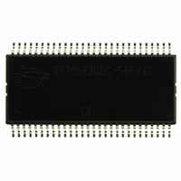
CY7C68300C-56PVXC Cypress Semiconductor Corp, CY7C68300C-56PVXC Datasheet - Page 41

CY7C68300C-56PVXC
Manufacturer Part Number
CY7C68300C-56PVXC
Description
IC USB 2.0 BRIDGE AT2LP 56-SSOP
Manufacturer
Cypress Semiconductor Corp
Series
CY7Cr
Type
USB to ATA/ATAPI Bridger
Datasheets
1.CY7C68300C-56PVXC.pdf
(42 pages)
2.CY7C68320C-100AXA.pdf
(44 pages)
3.CY7C68300C-56PVXC.pdf
(42 pages)
Specifications of CY7C68300C-56PVXC
Package / Case
56-SSOP
Controller Type
USB 2.0 Controller
Interface
I²C
Voltage - Supply
3.15 V ~ 3.45 V
Current - Supply
50mA
Operating Temperature
0°C ~ 70°C
Mounting Type
Surface Mount
Maximum Operating Temperature
+ 70 C
Minimum Operating Temperature
0 C
Mounting Style
SMD/SMT
Number Of Bits
48
Operating Temperature Range
0 C to + 70 C
Supply Current
10 mA
Operating Supply Voltage
3.3 V
Controller Family/series
(8051) USB
Core Size
8 Bit
No. Of I/o's
6
Embedded Interface Type
I2C, USB
Digital Ic Case Style
SSOP
Supply Voltage Range
3V To 3.6V
Rohs Compliant
Yes
Operating Temperature (min)
0C
Operating Temperature Classification
Commercial
Operating Temperature (max)
70C
Package Type
SSOP
Rad Hardened
No
Lead Free Status / RoHS Status
Lead free / RoHS Compliant
For Use With
CY4615B - KIT USB TO ATA REFERENCE DESIGN
Lead Free Status / Rohs Status
Lead free / RoHS Compliant
Other names
428-2266-5
CY7C68300C-56PVXC
CY7C68300C-56PVXC
Available stocks
Company
Part Number
Manufacturer
Quantity
Price
Company:
Part Number:
CY7C68300C-56PVXC
Manufacturer:
HITACHI
Quantity:
2 000
Company:
Part Number:
CY7C68300C-56PVXC
Manufacturer:
CY
Quantity:
8
Part Number:
CY7C68300C-56PVXC
Manufacturer:
CYPRESS/赛普拉斯
Quantity:
20 000
For further information on this package design, refer to the
application note Surface Mount Assembly of AMKOR’s
MicroLeadFrame (MLF) Technology. The application note
provides detailed information on board mounting guidelines,
soldering flow, rework process, and so on.
Figure 16
Other Design Considerations
Certain design considerations must be followed to ensure proper
operation of the CY7C68300C/CY7C68301C. The following
items must be taken into account when designing a USB device
with the CY7C68300C/CY7C68301C.
Proper Power Up Sequence
Power must be applied to the CY7C68300C/CY7C68301C
before, or at the same time as the ATA/ATAPI device. If power is
supplied to the drive first, the CY7C68300C/CY7C68301C
startup in an undefined state. Designs that use separate power
supplies for the CY7C68300C/CY7C68301C and the ATA/ATAPI
device are not recommended.
Document Number: 001-05809 Rev. *H
Figure 16. Plot of the Solder Mask (White Area)
is a plot of solder mask pattern and
Via hole for thermally connecting the
QFN to the circuit board ground plane.
PCB Material
Figure 15. Cross-Section of the Area Under the QFN Package
Figure 17
Cu Fill
displays an X-Ray image of assembly (darker areas indicate solder).
Solder Mask
0.013” dia
0.017” dia
Figure 15
package. The cross section is of only one via. The solder paste
template needs to be designed to enable at least 50% solder
coverage. The thickness of the solder paste template must be
5 mil. It is recommended that ’No Clean,’ type 3 solder paste is
used to mount the part. Nitrogen purge is recommended during
reflow.
IDE Removable Media Devices
The AT2LP does not fully support IDE removable media devices.
Changes in media state are not reported to the operating system
so users are unable to eject or reinsert media properly. This may
result in lost or corrupted data. Note that standard ATAPI optical
drives and ATA CompactFlash-type devices are not part of this
group.
Devices With Small Buffers
The size of the drive’s buffer can greatly affect the overall data
transfer performance. Ensure that drives have large enough
buffers to handle the flow of data to and from it. The exact buffer
size needed depends on a number of variables, but a good rule
of thumb to follow is:
(approx min buffer) = (data rate) * (seek time + rotation time + other)
where ’other’ may include things such as the time required to
switch heads and power up a laser. Drives with buffers that are
too small to handle the extra data may perform considerably
slower than expected.
This figure only shows the top three layers of the
circuit board: Top Solder, PCB Dielectric, and
the Ground Plane
Cu Fill
PCB Material
Figure 17. X-Ray Image of the Assembly
displays a cross-sectional area underneath the
CY7C68300C, CY7C68301C
CY7C68320C, CY7C68321C
Page 41 of 44
[+] Feedback


