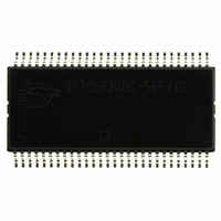
CY7C68300C-56PVXC Cypress Semiconductor Corp, CY7C68300C-56PVXC Datasheet - Page 13

CY7C68300C-56PVXC
Manufacturer Part Number
CY7C68300C-56PVXC
Description
IC USB 2.0 BRIDGE AT2LP 56-SSOP
Manufacturer
Cypress Semiconductor Corp
Series
CY7Cr
Type
USB to ATA/ATAPI Bridger
Datasheets
1.CY7C68300C-56PVXC.pdf
(42 pages)
2.CY7C68320C-100AXA.pdf
(44 pages)
3.CY7C68300C-56PVXC.pdf
(42 pages)
Specifications of CY7C68300C-56PVXC
Package / Case
56-SSOP
Controller Type
USB 2.0 Controller
Interface
I²C
Voltage - Supply
3.15 V ~ 3.45 V
Current - Supply
50mA
Operating Temperature
0°C ~ 70°C
Mounting Type
Surface Mount
Maximum Operating Temperature
+ 70 C
Minimum Operating Temperature
0 C
Mounting Style
SMD/SMT
Number Of Bits
48
Operating Temperature Range
0 C to + 70 C
Supply Current
10 mA
Operating Supply Voltage
3.3 V
Controller Family/series
(8051) USB
Core Size
8 Bit
No. Of I/o's
6
Embedded Interface Type
I2C, USB
Digital Ic Case Style
SSOP
Supply Voltage Range
3V To 3.6V
Rohs Compliant
Yes
Operating Temperature (min)
0C
Operating Temperature Classification
Commercial
Operating Temperature (max)
70C
Package Type
SSOP
Rad Hardened
No
Lead Free Status / RoHS Status
Lead free / RoHS Compliant
For Use With
CY4615B - KIT USB TO ATA REFERENCE DESIGN
Lead Free Status / Rohs Status
Lead free / RoHS Compliant
Other names
428-2266-5
CY7C68300C-56PVXC
CY7C68300C-56PVXC
Available stocks
Company
Part Number
Manufacturer
Quantity
Price
Company:
Part Number:
CY7C68300C-56PVXC
Manufacturer:
HITACHI
Quantity:
2 000
Company:
Part Number:
CY7C68300C-56PVXC
Manufacturer:
CY
Quantity:
8
Part Number:
CY7C68300C-56PVXC
Manufacturer:
CYPRESS/赛普拉斯
Quantity:
20 000
Additional Pin Descriptions
The following sections provide additional pin information.
DPLUS, DMINUS
DPLUS and DMINUS are the USB signaling pins; they must be
tied to the D+ and D– pins of the USB connector. Because they
operate at high frequencies, the USB signals require special
consideration when designing the layout of the PCB. See
General PCB Layout Recommendations for USB Mass Storage
Designs on page 40
When RESET# is released, the assertion of the internal pull up
on D+ is gated by a combination of the state of the
VBUS_ATA_ENABLE pin, the value of configuration address
0x08 bit 0 (DRVPWRVLD Enable), and the detection of a
non-removable ATA/ATAPI drive on the IDE bus. See
a description of this relationship.
Table 2. D+ Pull Up Assertion Dependencies
SCL, SDA
The clock and data pins for the I
the configuration EEPROM and to 2.2K pull up resistors tied to
V
must still be connected to pull up resistors. The SCL and SDA
pins are active for several milliseconds at startup.
XTALIN, XTALOUT
The AT2LP requires a 24 MHz (
internal timing. Typically, a 24 MHz (12 pF, 500 W,
parallel-resonant, fundamental mode) crystal is used, but a
24 MHz square wave (3.3 V, 50/50 duty cycle) from another
source can also be used. If a crystal is used, connect its pins to
XTALIN and XTALOUT, and also through 12 pF capacitors to
Table 3. Interrupt Data Bitmap
Document Number: 001-05809 Rev. *H
CC
ATA/ATAPI Drive Detected
DRVPWRVLD Enable Bit
7
. If no EEPROM is used in the design, the SCL and SDA pins
State of D+ pull up
6
VBUS_ATA_EN
5
for PCB layout recommendations.
EP1 Data Byte 1
4
Yes
1
1
1
2
C port must be connected to
3
100 ppm) signal to derive
No
1
1
1
Yes
1
0
1
2
No
1
0
0
1
Yes
0
1
0
Table 2
No
0
1
0
0
for
7
GND as shown in
apply it to XTALIN and leave XTALOUT unconnected.
SYSIRQ
The SYSIRQ pin provides a way for systems to request service
from host software by using the USB interrupt pipe on endpoint
1 (EP1). If the AT2LP has no pending interrupt data to return,
USB interrupt pipe data requests are NAK’ed. If pending data is
available, the AT2LP returns 16 bits of data. This data indicates
whether AT2LP is operating in high speed or full speed, whether
the AT2LP is reporting self powered or bus powered operation,
and the states of any GPIO pins that are configured as inputs.
GPIO pins can be individually set as inputs or outputs, with byte
0x09 of the configuration data. The state of any GPIO pin that is
not set as an input is reported as ‘0’ in the EP1 data.
Table 3
pipe and
incorporated by the AT2LP.
The SYSIRQ pin must be pulled LOW if HID functionality is used.
Refer to
details on HID functionality.
12pF
6
gives the bitmap for the data returned on the interrupt
HID Functions for Button Controls on page 15
Figure 7 on page 14
XTALIN
Figure 6. XTALIN/XTALOUT Diagram
5
CY7C68300C, CY7C68301C
CY7C68320C, CY7C68321C
Figure
EP1 Data Byte 0
4
24MHz Xtal
6. If an alternate clock source is used,
3
depicts the latching algorithm
2
XTALOUT
1
Page 13 of 44
0
for more
12pF
[+] Feedback


