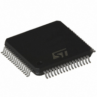
STLC5046 STMicroelectronics, STLC5046 Datasheet - Page 31

STLC5046
Manufacturer Part Number
STLC5046
Description
IC CODEC/FLTR PROG QUAD 64-TQFP
Manufacturer
STMicroelectronics
Type
PCM Codec/Filterr
Specifications of STLC5046
Data Interface
PCM Audio Interface
Resolution (bits)
16 b
Number Of Adcs / Dacs
4 / 4
Sigma Delta
Yes
Voltage - Supply, Analog
3.3 V ~ 5 V
Voltage - Supply, Digital
3.3 V ~ 5 V
Operating Temperature
-40°C ~ 85°C
Mounting Type
Surface Mount
Package / Case
64-TQFP, 64-VQFP
Lead Free Status / RoHS Status
Contains lead / RoHS non-compliant
Other names
497-3665
Available stocks
Company
Part Number
Manufacturer
Quantity
Price
Company:
Part Number:
STLC5046
Manufacturer:
ST
Quantity:
2 282
Part Number:
STLC5046
Manufacturer:
ST
Quantity:
20 000
Company:
Part Number:
STLC5046BCL
Manufacturer:
TOSHIBA
Quantity:
800
Company:
Part Number:
STLC5046BCP
Manufacturer:
ST
Quantity:
1 900
STLC5046
3.1.19
3.1.20
Receive Time Slot channel #0 (DRA0)
Addr=17h; Reset Value=00h
EN0=0: Disable reception of selected time slot.
EN0=1: Selected receive time slot on DR input is PCM decoded and transferred to VFRO0
output.
R06..0:Define receive time slot number (0 to 127) on carrying the PCM signal to be decoded
and transferred to VFRO0 output.If linear mode is selected (LIN=1 of CONF register) the 16
bits will be used as linear code as follows: the 8most significative bits in the programmed
time slot, the 8 least significative bits in the following timeslot.
Example: if R06..R00=00:
Pin-strap value (value 80h):
Referred to FS0.
Receive Time Slot channel #1 (DRA1)
Addr=18h; Reset Value=00h
EN1=0: Disable reception of selected time slot.
EN1=1: Selected receive time slot on DR input is PCM decoded and transferred to VFRO1
output.
R16..0:Define receive time slot number (0 to 127) on carrying the PCM signal to be decoded
and transferred to VFRO1 output.If linear mode is selected (LIN=1 of CONF register) the 16
bits will be used as linear code as follows: the 8most significative bits in the programmed
time slot, the 8 least significative bits in the following timeslot.
Example: if R16..R10=00:
15
EN0
EN0
Bit7
Bit7
1
14
13
Bit6
R06
Bit6
R16
0
12
TS0
11
Bit5
Bit5
R05
R15
0
10
Doc ID 7052 Rev 5
9
Bit4
R04
Bit4
R14
0
8
7
Bit3
R03
Bit3
R13
0
6
5
Bit2
Bit2
R02
R12
0
4
TS1
Registers addresses
3
Bit1
R01
Bit1
R11
0
2
1
Bit0
Bit0
R00
R10
0
31/51
0


