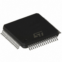
STLC5046 STMicroelectronics, STLC5046 Datasheet - Page 12

STLC5046
Manufacturer Part Number
STLC5046
Description
IC CODEC/FLTR PROG QUAD 64-TQFP
Manufacturer
STMicroelectronics
Type
PCM Codec/Filterr
Specifications of STLC5046
Data Interface
PCM Audio Interface
Resolution (bits)
16 b
Number Of Adcs / Dacs
4 / 4
Sigma Delta
Yes
Voltage - Supply, Analog
3.3 V ~ 5 V
Voltage - Supply, Digital
3.3 V ~ 5 V
Operating Temperature
-40°C ~ 85°C
Mounting Type
Surface Mount
Package / Case
64-TQFP, 64-VQFP
Lead Free Status / RoHS Status
Contains lead / RoHS non-compliant
Other names
497-3665
Available stocks
Company
Part Number
Manufacturer
Quantity
Price
Company:
Part Number:
STLC5046
Manufacturer:
ST
Quantity:
2 282
Part Number:
STLC5046
Manufacturer:
ST
Quantity:
20 000
Company:
Part Number:
STLC5046BCL
Manufacturer:
TOSHIBA
Quantity:
800
Company:
Part Number:
STLC5046BCP
Manufacturer:
ST
Quantity:
1 900
Functional description
2
2.1
2.2
2.3
12/51
Functional description
Power on initialization
When power is first applied it is recommended to reset the device by forcing the condition
M1.0=00, in order to clear all the internal registers.
In MCU mode M0 is set steadily Low and the device is reset by applying a negative pulse to
M1 (its operative level in MCU mode is High); same result can be obtained by writing an
High level into the control bit RES of the CONF register.
In pin-strap mode M1 is set steadily Low and the device is reset by applying a negative
pulse to M0 (its operative level in pin-strap mode is High); at the end of the Reset phase
(M0=High) the device is programmed according to the logical configuration of the control
pins.
During the reset condition all the I/On and CS_n pins are set as inputs, DX is set in high
impedance and all VFROn outputs are forced to AGND.
Power down state
Each of the four channel may be put into power down mode by setting the appropriate bit in
the CONF register or strapping to VDD the proper pin. In this mode the eventual
programmed DX channel is set in high impedance while the VFRO outputs are forced to
AGND. In pin-strap mode the value forced on the input pin is internally updated every FS
signal.
Transmit path
The analog VFXI signal through an amplifier stage is applied to a PCM converter and the
corresponding digital signal is sent to DX output.
In MCU mode, the amplifier gain can be programmed with two different values by means of
TXG Reg.: 0 dB or +3.52 dB.
A programmable gain block after the A/D conversion allows to set transmit gain in 12dB
range, with steps <0.1dB by writing proper code into GTXn register.
Setting GTXn=00h, the transmitted signal is muted, i.e. an idle PCM signal is generated on
DX.
A/µ coding Law is selected by bit5 (AMU) of CONF reg.
Setting LIN=1 (bit6 of CONF reg.) the linear coding Law is selected (16bits); in this case the
signal sent on DX will take two adjacent PCM time slots.
In Pin-strap mode, the amplifier gain is set to 0dB; only two values of Transmit gain can be
selected according to the level of GXn control input (in Pin-strap):
GXn=1 selects the gain corresponding to GTXn=FFh (0 dB)
GXn=0 selects the gain corresponding to GTXn=8Fh (-3.5 dB)
Different gain value is obtained through proper voltage divider.
A/µ coding Law is selected according to AMU pin level:
Doc ID 7052 Rev 5
STLC5046


