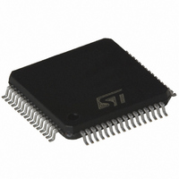
STLC5046 STMicroelectronics, STLC5046 Datasheet - Page 14

STLC5046
Manufacturer Part Number
STLC5046
Description
IC CODEC/FLTR PROG QUAD 64-TQFP
Manufacturer
STMicroelectronics
Type
PCM Codec/Filterr
Specifications of STLC5046
Data Interface
PCM Audio Interface
Resolution (bits)
16 b
Number Of Adcs / Dacs
4 / 4
Sigma Delta
Yes
Voltage - Supply, Analog
3.3 V ~ 5 V
Voltage - Supply, Digital
3.3 V ~ 5 V
Operating Temperature
-40°C ~ 85°C
Mounting Type
Surface Mount
Package / Case
64-TQFP, 64-VQFP
Lead Free Status / RoHS Status
Contains lead / RoHS non-compliant
Other names
497-3665
Available stocks
Company
Part Number
Manufacturer
Quantity
Price
Company:
Part Number:
STLC5046
Manufacturer:
ST
Quantity:
2 282
Part Number:
STLC5046
Manufacturer:
ST
Quantity:
20 000
Company:
Part Number:
STLC5046BCL
Manufacturer:
TOSHIBA
Quantity:
800
Company:
Part Number:
STLC5046BCP
Manufacturer:
ST
Quantity:
1 900
Functional description
2.5
2.5.1
14/51
In MCU mode a programmable gain block before the A/D conversion allows to set receive
gain in 12dB range, with steps <0.1 dB by writing proper code into GRXn register.
The amplifier gain can be programmed with five different values by means of RXG register:
0 dB -1.94 dB -4.44 dB -7.96 dB -13.98 dB.
Setting GRXn=00h, the receive signal is muted and VFRO output is set to AGND.
A/µ coding Law is selected by bit5 (AMU) of CONF reg.
Setting LIN = 1 (bit6 of CONF reg.) the linear coding Law is selected (16bits); in this case
the signal received on DR will take two adjacent PCM time slots.
In pin-strap mode only two values of Receive Gain can be selected according to the level of
GRn control input (in pin-strap) GRn = 1 selects the gain corresponding to GRXn= E2h,
RXG = 0dB (-0.8 dB) GRn = 0 selects the gain corresponding to GRXn = AFh,
RXG = -1.94 dB (-4.3 dB).
Different gain value is obtained through proper voltage divider.
A/µ coding Law is selected according to AMU pin level:
AMU=0 µ Law selected.
AMU=1 A Law selected.
VFRO output, referred to AGND must be AC coupled to the load, referred to VSS, to prevent
a DC current flow.
VFRO has a drive capability of 1.0mA (peak value), with a max AC swing of 2 Vpp.
In order to get the best noise performances it is recommended to keep the GRX value as
close as possible to the maximum (FFh) setting properly the additional attenuation by
means of RXG.
PCM interface
The STLC5046 dedicate five pins (six in pin-strap mode) to the interface with the PCM
highways.
MCLK represents the bit clock and is also used by the device as a source for the clock of the
internal Sigma Delta converter timings. Four possible frequencies can be used:
1.536/1.544 MHz (24 channels PCM frame); 2048 MHz (32 channels PCM frame);
4.096 MHz (64 channels PCM frame); 8.192 MHz (128 channels PCM frame).
The operating frequency is automatically detected by the device when both MCLK and FS
are applied. MCLK is synchronizing both the transmit data (DX) and the receive data (DR).
MCU mode
The Frame Sync. signal FS is the common time base for all the four channels; Short (one
MCLK period) or Long (more than one MCLK period) FS are allowed.
Transmit and Receive programmable Time-Slots are framed to an internal sync. signal that
can be coincident with FS or delayed of 1 to 7 MCLK cycles depending on the programming
of PCMSH register.
Doc ID 7052 Rev 5
STLC5046


