UDA1338H/N1,518 NXP Semiconductors, UDA1338H/N1,518 Datasheet
UDA1338H/N1,518
Specifications of UDA1338H/N1,518
UDA1338HB-T
UDA1338HB-T
Available stocks


Related parts for UDA1338H/N1,518


UDA1338H/N1,518 Summary of contents
Page 1
UDA1338H Multichannel audio coder-decoder Rev. 04 — 18 May 2010 1. General description The UDA1338H is a single-chip consisting of 4 plus 1 analog-to-digital converters and 6 digital-to-analog converters with signal processing features employing bitstream conversion techniques. The multichannel configuration ...
Page 2
... NXP Semiconductors 2.2 Multiple format data interface Audio interface supports standard I multichannel formats Voice interface supports I 2.3 Digital sound processing Control via L3-bus or I Channel independent digital logarithmic volume Digital de-emphasis for f Soft or quick mute Output signal polarity control 2.4 Advanced audio configuration Inputs: 4 single-ended audio inputs (2 × ...
Page 3
... NXP Semiconductors Table DDD (pins V SS Symbol I DDD(pd) T amb Audio analog-to-digital converter D 0 (THD+N)/S total harmonic S/N α cs Digital-to-analog converter Differential mode V o(rms) (THD+N)/S total harmonic S/N α cs Single-ended mode V o(rms) (THD+N)/S total harmonic S/N α cs [1] The input voltage can (RMS) when the current through the ADC input pin is limited to approximately using a series resistor ...
Page 4
... NXP Semiconductors 6. Block diagram VINL1 VINL2 VVOICE DATAV BCKV WSV MCCLK MCMODE MCDATA I2C_L3 VOUT1N VOUT1P VOUT3N VOUT3P VOUT5N VOUT5P Fig 1. Block diagram UDA1338H Product data sheet V DDA(AD PGA ADC 1L 6 ADC 2L PGA 10 LNA DECIMATION FILTER ADC DC-CANCELLATION FILTER DECIMATION FILTER ...
Page 5
... NXP Semiconductors 7. Pinning information 7.1 Pinning Fig 2. Pin configuration 7.2 Pin description Table 3: Symbol V ref VINL1 V SSA(AD) VINR1 V DDA(AD) VINL2 V ADCN VINR2 V ADCP VVOICE TEST DATAAD2 DATAAD1 BCKAD WSAD UDA1338H Product data sheet V 1 ref VINL1 SSA(AD) 4 VINR1 V 5 DDA(AD) UDA1338H ...
Page 6
... NXP Semiconductors Table 3: Symbol DATAV BCKV WSV SYSCLK MCMODE MCCLK MCDATA WSDA BCKDA DATADA1 DATADA2 DATADA3 V SSD V DDD I2C_L3 VOUT1P VOUT1N VOUT2P VOUT2N VOUT3P VOUT3N V DDA(DA) VOUT4P VOUT4N V SSA(DA) VOUT5P VOUT5N VOUT6P VOUT6N [1] See Table 4: Type AGND AIO AS DGND DI DID DIO ...
Page 7
... NXP Semiconductors Table 4: Type DIS DO DS IIC 8. Functional description 8.1 System clock The UDA1338H operates in slave mode only; this means that in all applications the system must provide either the system clock (the bit clock for the voice ADC) or the word clock. ...
Page 8
... NXP Semiconductors Table 6: Mode WSV-in WSV-out 8.2 Audio analog-to-digital converter (audio ADC) The audio analog-to-digital front-end of the UDA1338H consists of 4-channel single-ended Adds with programmable gain stage (from with 3 dB steps), controlled via the microcontroller interface. Using the PGA feature possible to accept an input signal of 900 mV (RMS) or 1.8 V (RMS external resistor of 10 kΩ ...
Page 9
... NXP Semiconductors 8.5 Decimation filter of voice ADC The voice ADC decimation filter is realized with the combination of a Finite Impulse Response (FIR) filter and Infinite Impulse Response (IIR) filter for shorter group delay. The filter characteristics are shown in of the ADC is hard muted for a certain period. This hard-mute time can be chosen between 1024 and 2048 samples ...
Page 10
... NXP Semiconductors MIX [ 1:0 ] from ADC ch1 ch2 ch3 ch4 2 from I S-bus DATADA1 DATADA2 DATADA3 DIS [ 1:0 ] ICS [ 1:0 ] Fig 4. Block diagram of DAC mixer 8.9 Audio digital-to-analog converters The audio digital-to-analog front-end of the UDA1338H consists of 6-channel differential SDACs: an SDAC is a multi-bit DAC based upon switched resistors. To minimize data dependent modulation effects, a Dynamic Element Matching (DEM) algorithm scrambler circuit and DC current compensation circuit are implemented with the SDAC ...
Page 11
... NXP Semiconductors Fig 5. Power-on reset circuit Fig 6. Power-on reset timing 8.11 Audio digital interface The following audio formats can be selected via the microcontroller interface: • S-bus format with data word length bits • MSB-justified format with data word length bits • ...
Page 12
LEFT WS > BCK DATA MSB S-BUS FORMAT WS LEFT BCK DATA MSB B2 LSB MSB-JUSTIFIED FORMAT WS LEFT BCK DATA WS LEFT 20 19 BCK DATA MSB B2 ...
Page 13
BCK DATA MSB LSB MSB CH1 CH3 BCK DATA MSB LSB MSB CH1 CH3 BCK DATA MSB LSB MSB CH1 (1) Format 1. (2) ...
Page 14
... NXP Semiconductors 8.12 Voice digital interface The following voice formats can be selected via the microcontroller interface: • S-bus format with data word length bits. The left and the right channels contain the same data. • Mono channel format with data word length bits ...
Page 15
... NXP Semiconductors 8.14 Microcontroller interface mode The microcontroller interface mode can be selected as shown in • L3-bus mode when pin I2C_L3 = LOW • C-bus mode when pin I2C_L3 = HIGH Table 11. Pin MCCLK MCDATA MCMODE Table 12: Signal QMUTE LOW HIGH All the features are accessible with the I interface protocol ...
Page 16
... NXP Semiconductors The data transfer mode is characterized by signal L3MODE = HIGH and is used to transfer one or more bytes representing a register address, instruction or data. Basically, two types of data transfers can be defined: • Write action: data transfer to the device • Read action: data transfer from the device. ...
Page 17
L3CLOCK L3MODE device address 0 1 L3DATA DOM bits Fig 11. Data write mode L3CLOCK L3MODE device address register address L3DATA DOM bits read prepare read Fig 12. Data read mode register address data byte 1 0 ...
Page 18
... NXP Semiconductors 9.4 Data write mode The data write mode is explained in the signal diagram of device, 4 bytes must be sent (see 1. Byte 1 starting with ‘01’ for signalling the write action to the device, followed by the device address ‘01 0100’. 2. Byte 2 starting with a ‘0’ for signalling the write action, followed by 7 bits indicating the destination address in binary format with bit A6 being the MSB and bit A0 being the LSB ...
Page 19
... NXP Semiconductors Table 15: Byte L3-bus mode 1 address 2 data transfer register address 3 address 4 data transfer register address 5 data transfer data byte 1 6 data transfer data byte 2 2 10. I C-bus interface 10.1 General The UDA1338H has an I with the I accessible via pin MCMODE with signal QMUTE. ...
Page 20
... NXP Semiconductors 10.4 Byte transfer Each byte (8 bits) is transferred with the MSB first; see Table 16: MSB 7 10.5 Data transfer A device generating a message is a transmitter; a device receiving a message is the receiver. The device that controls the message is the master and the devices which are controlled by the master are the slaves ...
Page 21
... NXP Semiconductors SDA SCL Fig 14. START and STOP conditions on the I Fig 15. Acknowledge on the I 10.8 Device address Before any data is transmitted on the I addressed first. The addressing is always done with byte 1 transmitted after the start procedure. The UDA1338H acts as a slave receiver or a slave transmitter. ...
Page 22
... NXP Semiconductors 10.10 Write and read data 2 The I C-bus configurations for a write and read cycle are shown in respectively. The write cycle is used to write groups of two bytes to the internal registers for the settings also possible to read the registers for the device status information. ...
Page 23
... NXP Semiconductors 4. After this the microcontroller writes the 8-bit register address (ADDR) where the reading of the register content of the UDA1338H must start. 5. The UDA1338H acknowledges this register address. 6. Then the microcontroller generates a repeated start (Sr). 7. Then the microcontroller generates the device address ‘0011 000’ again, but this time followed by a logic 1 (read) of the R/W bit ...
Page 24
... NXP Semiconductors Table 20: Address 12h 13h 14h 15h 16h 17h 18h 19h 1Ah 1Bh 1Ch 1Dh ADC input amplifier gain settings 20h 21h Supplemental settings 30h 31h UDA1338H Product data sheet Overview of register mapping …continued All information provided in this document is subject to legal disclaimers. ...
Page 25
Register mapping [1] Table 21: UDA1338H register mapping Add Function D15 D14 D13 D12 System settings [2] 00h system RST VFS1 VFS0 VCE - 01h audio ADC DC PAB PAA MTB and DAC ...
Page 26
Table 21: UDA1338H register mapping …continued Add Function D15 D14 D13 D12 19h DAC mixing - - - - channel 1Ah DAC mixing ICS1 ICS0 - - channel 1Bh ...
Page 27
... NXP Semiconductors 11.3 System settings Table 22: Bit Symbol Reset default Bit Symbol Reset default Table 23: Bit UDA1338H Product data sheet System register (address 00h RST VFS1 VFS0 - OP1 OP0 FS1 Description of system register bits Symbol Description RST Reset. A 1-bit value to initialize the L3-bus registers with the default settings by writing bit RST = 1 ...
Page 28
... NXP Semiconductors Table 24: VFS1 Table 25: SC1 Table 26: OP1 Table 27: FS1 11.4 Audio ADC and DAC subsystem settings Table 28: Bit Symbol Reset default Bit Symbol Reset default UDA1338H Product data sheet Voice ADC sampling frequency bits VFS0 System clock frequency bits SC0 ...
Page 29
... NXP Semiconductors Table 29: Bit Table 30: AIF2 DIF2 UDA1338H Product data sheet Description of the audio ADC and DAC subsystem register bits Symbol Description DC ADC DC-filter. A 1-bit value to enable the digital DC-filter of the ADC. If bit (default), then the DC-filtering is active; if bit then there is no DC-filtering ...
Page 30
... NXP Semiconductors Table 31: DIS1 11.5 Voice ADC system settings Table 32: Bit Symbol Reset default Bit Symbol Reset default Table 33: Bit Table 34: BCK1 UDA1338H Product data sheet Data interface selection bits DIS0 Input to DAC 0 DATADA1 to DAC channel 1 and channel 2, DATADA2 to DAC channel 3 ...
Page 31
... NXP Semiconductors Table 35: VH1 11.6 Status output register (read only) Table 36: Bit Symbol Bit Symbol Table 37: Bit UDA1338H Product data sheet Voice ADC high-pass filter setting bits VH0 Status output register (address 0Fh Description of status output register bits Symbol Description - not used VS Voice ADC status ...
Page 32
... NXP Semiconductors 11.7 DAC channel selection Table 38: Bit Symbol Reset default Bit Symbol Reset default Table 39: Bit and Table 40: MIX1 Table 41: MC5 CS5 UDA1338H Product data sheet DAC channel select register (address 10h MIX1 MIX0 MC5 SEL1 SEL0 CS5 Description of DAC channel select register bits ...
Page 33
... NXP Semiconductors Table 42: SEL1 11.8 DAC features settings Table 43: Bit Symbol Reset default Bit Symbol Reset default Table 44: Bit UDA1338H Product data sheet Feature selection bits SEL0 DAC features register (addresses 11h ICS1 ICS0 DE2 VC7 VC6 VC5 Description of DAC features register bits ...
Page 34
... NXP Semiconductors Table 45: ICS1 Table 46: DE2 Table 47: VC7 UDA1338H Product data sheet Input channel selection bits ICS0 Input to DAC output 0 left channel input data to odd channel output; right channel input data to even channel output 1 left channel input data to odd and even channel outputs ...
Page 35
... NXP Semiconductors 11.9 DAC channel 1 to channel 6 settings All the DAC features which are written in register 11h are copied into the odd channel registers. Table 48: Bit Symbol Reset default Bit Symbol Reset default All the DAC features which are written in register 11h are copied into the even channel registers, except the bits ICS[1:0] ...
Page 36
... NXP Semiconductors Table 51: Bit Symbol Reset default Bit Symbol Reset default 11.11 Audio ADC 1 and ADC 2 input amplifier gain settings Table 52: Bit Symbol Reset default Bit Symbol Reset default Table 53: Bit Table 54: IA3 IB3 UDA1338H Product data sheet DAC mixing channel 2, 4 and 6 registers (addresses 19h, 1Bh and 1Dh) ...
Page 37
... NXP Semiconductors 11.12 Voice ADC gain settings Table 55: Bit Symbol Reset default Bit Symbol Reset default Table 56: Bit Table 57: IV4 11.13 Supplemental settings 1 Table 58: Bit Symbol Reset default Bit Symbol Reset default UDA1338H Product data sheet Voice ADC input amplifier gain register (address 21h) ...
Page 38
... NXP Semiconductors Table 59: Bit 11.14 Supplemental settings 2 Table 60: Bit Symbol Reset default Bit Symbol Reset default Table 61: Bit Table 62: DITH2 UDA1338H Product data sheet Description of supplemental settings 1 register bits Symbol Description - default 0000 0000 PDT Power-down time. A 1-bit value to select the time of the SDAC power-down sequence ...
Page 39
... NXP Semiconductors 12. Limiting values Table 63: In accordance with the Absolute Maximum Rating System (IEC 60134). Symbol Parameter xtal(max) T stg T amb V esd [1] All supply connections must be made to the same power supply. [2] Equivalent to discharging a 100 pF capacitor via a 1.5 kΩ series resistor. Equivalent to discharging a 200 pF capacitor via a 0.75 μH series inductor. ...
Page 40
... NXP Semiconductors 14. Static characteristics Table 65: DC characteristics 3 DDD DDA(AD) DDA(DA) specified. Symbol Parameter Supplies V ADC analog supply DDA(AD) voltage V DAC analog supply DDA(DA) voltage V digital supply voltage DDD I ADC analog supply DDA(AD) current I DAC analog supply DDA(DA) current I digital supply current ...
Page 41
... NXP Semiconductors Table 65: DC characteristics …continued 3 DDD DDA(AD) DDA(DA) specified. Symbol Parameter R input resistance of i(VADC) voice ADC Digital-to-analog converter R load resistance L R output resistance o [1] All supply connections must be made to the same power supply unit. 15. Dynamic characteristics Table 66: AC characteristics 3 DDD ...
Page 42
... NXP Semiconductors Table 66: AC characteristics …continued 3 DDD DDA(AD) DDA(DA) referenced to ground (pins V ); unless otherwise specified. SS Symbol Parameter (THD + N)/S total harmonic distortion-plus-noise to signal ratio S/N signal-to-noise ratio α channel separation cs Voice analog-to-digital converter V input voltage (RMS value) i(rms) (THD + N)/S total harmonic ...
Page 43
... NXP Semiconductors Table 66: AC characteristics …continued 3 DDD DDA(AD) DDA(DA) referenced to ground (pins V ); unless otherwise specified. SS Symbol Parameter Single-ended mode V output voltage (RMS value) o(rms) ΔV output voltage unbalance o between channels (THD + N)/S total harmonic distortion-plus-noise to signal ratio S/N signal-to-noise ratio α ...
Page 44
... NXP Semiconductors Table 67: Timing …continued 2 3 DDD DDA(AD) DDA(AD kHz; unless otherwise specified. s Symbol Parameter t data input hold time h(DATAI) t data output hold time h(DATAO) t data output to bit clock delay d(DATAO-BCK) t data output to word select delay d(DATAO-WS) Serial data of voice ADC ...
Page 45
... NXP Semiconductors Table 67: Timing …continued 2 3 DDD DDA(AD) DDA(AD kHz; unless otherwise specified. s Symbol Parameter 2 I C-bus interface timing; see Figure 20 SCL timing f SCL clock frequency SCL t SCL LOW time LOW t SCL HIGH time HIGH t rise time SDA and SCL r t fall time SDA and SCL ...
Page 46
... NXP Semiconductors WS t BCKH t r BCK T DATAO DATAI 2 Fig 17. I S-bus serial interface timing L3MODE L3CLOCK L3DATA Fig 18. L3-bus address mode timing UDA1338H Product data sheet t t h(WS BCKL t d(DATAO-WS) cy(BCK) t h(L3)A t CLK(L3 CLK(L3)H su(L3)A t su(L3)DA BIT 0 All information provided in this document is subject to legal disclaimers. ...
Page 47
... NXP Semiconductors L3MODE t su(L3)D L3CLOCK L3DATA write L3DATA read t en(L3)R Fig 19. L3-bus data transfer (write and read) mode timing SDA LOW r SCL t HD;STA t HD;DAT S 2 Fig 20. I C-bus timing UDA1338H Product data sheet t CLK(L3)L t CLK(L3)H t su(L3)DA t h(L3)DA BIT 0 t h(L3 SU;DAT t SU ...
Page 48
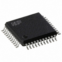
... NXP Semiconductors 17. Package outline QFP44: plastic quad flat package; 44 leads (lead length 1.3 mm); body 1. pin 1 index DIMENSIONS (mm are the original dimensions) A UNIT max. 0.25 1.85 mm 2.1 0.25 0.05 1.65 Note 1. Plastic or metal protrusions of 0.25 mm maximum per side are not included. OUTLINE ...
Page 49
... NXP Semiconductors 18. Handling information All input and output pins are protected against ElectroStatic Discharge (ESD) under normal handling. When handling ensure that the appropriate precautions are taken as described in JESD625-A or equivalent standards. 19. Soldering of SMD packages This text provides a very brief insight into a complex technology. A more in-depth account of soldering ICs can be found in Application Note AN10365 “ ...
Page 50
... NXP Semiconductors • Process issues, such as application of adhesive and flux, clinching of leads, board transport, the solder wave parameters, and the time during which components are exposed to the wave • Solder bath specifications, including temperature and impurities 19.4 Reflow soldering Key characteristics in reflow soldering are: • ...
Page 51
... NXP Semiconductors Fig 22. Temperature profiles for large and small components For further information on temperature profiles, refer to Application Note AN10365 “Surface mount reflow soldering description”. UDA1338H Product data sheet maximum peak temperature = MSL limit, damage level temperature minimum peak temperature = minimum soldering temperature MSL: Moisture Sensitivity Level All information provided in this document is subject to legal disclaimers ...
Page 52
... Modifications: The format of this data sheet has been redesigned to comply with the new identity guidelines of NXP Semiconductors. • Legal texts have been adapted to the new company name where appropriate. • Section “Test information” and subsection “Quality information” removed. ...
Page 53
... In no event shall NXP Semiconductors be liable for any indirect, incidental, punitive, special or consequential damages (including - without limitation - lost profits, lost savings, business interruption, costs related to the removal or ...
Page 54
... NXP Semiconductors’ specifications such use shall be solely at customer’s own risk, and (c) customer fully indemnifies NXP Semiconductors for any liability, damages or failed product claims resulting from customer design and use of the product for automotive applications beyond NXP Semiconductors’ ...
Page 55
... NXP Semiconductors 23. Contents 1 General description . . . . . . . . . . . . . . . . . . . . . . 1 2 Features and benefits . . . . . . . . . . . . . . . . . . . . 1 2.1 General . . . . . . . . . . . . . . . . . . . . . . . . . . . . . . . 1 2.2 Multiple format data interface . . . . . . . . . . . . . . 2 2.3 Digital sound processing 2.4 Advanced audio configuration . . . . . . . . . . . . . 2 3 Applications . . . . . . . . . . . . . . . . . . . . . . . . . . . . 2 4 Quick reference data . . . . . . . . . . . . . . . . . . . . . 2 5 Ordering information . . . . . . . . . . . . . . . . . . . . . 3 6 Block diagram . . . . . . . . . . . . . . . . . . . . . . . . . . 4 7 Pinning information . . . . . . . . . . . . . . . . . . . . . . 5 7.1 Pinning . . . . . . . . . . . . . . . . . . . . . . . . . . . . . . . 5 7 ...