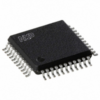
UDA1338H/N1,518 NXP Semiconductors, UDA1338H/N1,518 Datasheet - Page 22

UDA1338H/N1,518
Manufacturer Part Number
UDA1338H/N1,518
Description
IC AUDIO CODER/DECODER 44QFP
Manufacturer
NXP Semiconductors
Type
Stereo Audior
Datasheet
1.UDA1338HN1518.pdf
(55 pages)
Specifications of UDA1338H/N1,518
Package / Case
44-MQFP, 44-PQFP
Data Interface
Serial
Resolution (bits)
24 b
Number Of Adcs / Dacs
5 / 6
Sigma Delta
No
S/n Ratio, Adcs / Dacs (db) Typ
100 / 114
Voltage - Supply, Analog
2.7 V ~ 3.6 V
Voltage - Supply, Digital
2.7 V ~ 3.6 V
Operating Temperature
-20°C ~ 85°C
Mounting Type
Surface Mount
Product
General Purpose Audio Amplifiers
Available Set Gain
26 dB
Operating Supply Voltage
3.3 V
Supply Current
30 mA, 20 mA, 31 mA
Maximum Operating Temperature
+ 85 C
Mounting Style
SMD/SMT
Audio Load Resistance
22 KOhms
Input Signal Type
Single
Minimum Operating Temperature
- 20 C
Output Signal Type
Differential
Supply Voltage (max)
3.6 V
Supply Voltage (min)
2.7 V
Output Type
Differential
Lead Free Status / RoHS Status
Lead free / RoHS Compliant
Lead Free Status / RoHS Status
Lead free / RoHS Compliant, Lead free / RoHS Compliant
Other names
935268945518
UDA1338HB-T
UDA1338HB-T
UDA1338HB-T
UDA1338HB-T
Available stocks
Company
Part Number
Manufacturer
Quantity
Price
Company:
Part Number:
UDA1338H/N1,518
Manufacturer:
NXP Semiconductors
Quantity:
10 000
NXP Semiconductors
Table 18.
[1]
UDA1338H
Product data sheet
S
Auto increment of register address.
Device
address
0011 000
acknowledge from UDA1338H
Master transmitter writes to UDA1338H registers in the I
10.10 Write and read data
10.12 Read cycle
10.11 Write cycle
R/
W
0
A
The I
respectively.
The write cycle is used to write groups of two bytes to the internal registers for the
settings. It is also possible to read the registers for the device status information.
The I
write the data to the internal registers. The device and register addresses are one byte
each, the setting data is always a pair of two bytes.
The format of the write cycle is as follows:
The read cycle is used to read the data values from the internal registers. The I
configuration for a read cycle is shown in
The format of the read cycle is as follows:
1. The microcontroller starts with a start condition (S).
2. The first byte (8 bits) contains the device address ‘0011 000’ and a logic 0 (write) for
3. This is followed by an acknowledge (A) from the UDA1338H.
4. After this the microcontroller writes the 8-bit register address (ADDR) where the
5. The UDA1338H acknowledges this register address (A).
6. The microcontroller sends 2 bytes data with the Most Significant (MS) byte first and
7. If repeated groups of 2 bytes data are transmitted, then the register address is auto
8. Finally, the UDA1338H frees the I
1. The microcontroller starts with a start condition (S).
2. The first byte (8 bits) contains the device address ‘0011 000’ and a logic 0 (write) for
3. This is followed by an acknowledge (A) from the UDA1338H.
Register
address
ADDR
the R/W bit.
writing of the register content of the UDA1338H must start.
then the Least Significant (LS) byte. After each byte an acknowledge is followed from
the UDA1338H.
incremented. After each byte an acknowledge is followed from the UDA1338H.
condition (P).
the R/W bit.
2
2
C-bus configurations for a write and read cycle are shown in
C-bus configuration for a write cycle is shown in
A
All information provided in this document is subject to legal disclaimers.
data 1
MS1
Rev. 04 — 18 May 2010
A
LS1
A
2
C-bus and the microcontroller can generate a stop
DATA 2
MS2
Table
2
C-bus mode
[1]
19.
A
LS2
Multichannel audio coder-decoder
Table
A
18. The write cycle is used to
DATA n
MSn
Table 18
UDA1338H
[1]
A
© NXP B.V. 2010. All rights reserved.
LSn
and
2
Table
C-bus
A
22 of 55
19,
P


