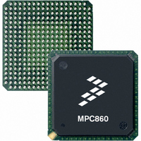
MC68360ZP25L Freescale Semiconductor, MC68360ZP25L Datasheet - Page 311

MC68360ZP25L
Manufacturer Part Number
MC68360ZP25L
Description
IC MPU QUICC 25MHZ 357-PBGA
Manufacturer
Freescale Semiconductor
Datasheets
1.MC68EN360VR25L.pdf
(14 pages)
2.MC68EN360VR25L.pdf
(2 pages)
3.MC68360AI25L.pdf
(962 pages)
Specifications of MC68360ZP25L
Processor Type
M683xx 32-Bit
Speed
25MHz
Voltage
5V
Mounting Type
Surface Mount
Package / Case
357-PBGA
Lead Free Status / RoHS Status
Contains lead / RoHS non-compliant
Features
-
Available stocks
Company
Part Number
Manufacturer
Quantity
Price
Company:
Part Number:
MC68360ZP25L
Manufacturer:
Freescale Semiconductor
Quantity:
10 000
Company:
Part Number:
MC68360ZP25LR2
Manufacturer:
PMC
Quantity:
95
Company:
Part Number:
MC68360ZP25LR2
Manufacturer:
Freescale Semiconductor
Quantity:
10 000
Part Number:
MC68360ZP25LR2
Manufacturer:
FREESCALE
Quantity:
20 000
- Current page: 311 of 962
- Download datasheet (4Mb)
EMWS—External Master Wait State (SRAM Bank Only)
The following bits are used for both DRAM and SRAM memory:
SYNC—Synchronous External Access MC68030-Type
This attribute should be set if an additional wait state is necessary when an asynchronous
external MC68030-type device or external QUICC is accessing SRAM banks (see Table
6-11). This bit is only used if SYNC = 0.
This attribute applies only to an external MC68030-type device or external QUICC that
uses the on-chip memory controller. It determines how the memory controller will assert
its signals in response to what it sees from the external master.
When the SRAM controller is used, CS and DSACK assertion and negation timings are
asynchronous. They are asserted and negated in relation to the external master’s AS line.
The CSNTQ and the TRLXQ attributes are ignored. When EMWS is set, one wait state is
added to the programmed TCYC.
When the DRAM controller is used, CAS and DSACK are negated asynchronously with
the negation of the external master’s AS.
0 = Normal operation.
1 = Insert one additional wait state for external QUICC/MC68030-type masters on their
0 = Asynchronous operation of the memory controller (external MC68030-type master
accesses to all SRAM banks.)
only).
chronous to the QUICC clock. When asynchronous external
masters are using the DRAM controller, the BSTM bit in the
MCR should be cleared.
The DRAM controller’s assertion of RAS and CAS is always syn-
0
1
2
3
4
5
6
15
NOTE: The BSTM bit is located in the MCR of the SI60.
TCYC =
Table 6-11. External MC68030-Type Cycle Length
…
(SRAM Bank in Asynchronous Operation
Freescale Semiconductor, Inc.
For More Information On This Product,
Synchronous Bus Timing
EMWS = 0
External QUICC/MC68030-Type Bus Cycle Length
17
…
3
3
4
5
6
7
8
MC68360 USER’S MANUAL
(BSTM = 1)
Go to: www.freescale.com
EMWS = 1
NOTE
18
…
3
4
5
6
7
8
9
Asynchronous Bus Timing
EMWS = 0
18
…
3
3
5
6
7
8
9
(BSTM = 0)
System Integration Module (SIM60)
EMWS = 1
10
19
…
3
5
6
7
8
9
Related parts for MC68360ZP25L
Image
Part Number
Description
Manufacturer
Datasheet
Request
R
Part Number:
Description:
Manufacturer:
Freescale Semiconductor, Inc
Datasheet:

Part Number:
Description:
MC68360 MC68360 Multiple Ethernet Channels on the QUICC
Manufacturer:
Motorola / Freescale Semiconductor

Part Number:
Description:
MC68360 Implementing an 8 bit Eprom for an MC68EC040-MC68360 System
Manufacturer:
Motorola / Freescale Semiconductor

Part Number:
Description:
MC68360 Interfacing the MC68060 to the MC68360
Manufacturer:
Motorola / Freescale Semiconductor

Part Number:
Description:
MC68360 MC68360 RAM Microcode Package Option Overview
Manufacturer:
Motorola / Freescale Semiconductor

Part Number:
Description:
MC68360 MC68360 CPM-CPU Interaction
Manufacturer:
Motorola / Freescale Semiconductor

Part Number:
Description:
MC68360 Interfacing SDRAM to the MC68360 QUICC Device
Manufacturer:
Motorola / Freescale Semiconductor

Part Number:
Description:
MC68360 Interfacing the QUICC to a MCM516400 (4Mx4 10-12 column-row) DRAM
Manufacturer:
Motorola / Freescale Semiconductor

Part Number:
Description:
MC68360 Interfacing the 68360 (QUICC) to T1-E1 Systems
Manufacturer:
Motorola / Freescale Semiconductor

Part Number:
Description:
MC68360 Multiple QUICC Design Concept
Manufacturer:
Motorola / Freescale Semiconductor
Part Number:
Description:
Manufacturer:
Freescale Semiconductor, Inc
Datasheet:
Part Number:
Description:
Manufacturer:
Freescale Semiconductor, Inc
Datasheet:
Part Number:
Description:
Manufacturer:
Freescale Semiconductor, Inc
Datasheet:
Part Number:
Description:
Manufacturer:
Freescale Semiconductor, Inc
Datasheet:
Part Number:
Description:
Manufacturer:
Freescale Semiconductor, Inc
Datasheet:


