MC68EC020FG25 Freescale Semiconductor, MC68EC020FG25 Datasheet - Page 61
MC68EC020FG25
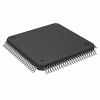
Manufacturer Part Number
MC68EC020FG25
Description
IC MPU 32 BIT 25MHZ 100-QFP
Manufacturer
Freescale Semiconductor
Datasheet
1.MC68EC020AA16.pdf
(306 pages)
Specifications of MC68EC020FG25
Processor Type
M680x0 32-Bit
Speed
25MHz
Voltage
5V
Mounting Type
Surface Mount
Package / Case
100-QFP
Lead Free Status / RoHS Status
Contains lead / RoHS non-compliant
Features
-
Available stocks
Company
Part Number
Manufacturer
Quantity
Price
Company:

Part Number:
MC68EC020FG25
Manufacturer:
FREESCALE
Quantity:
8 831
Company:
Part Number:
MC68EC020FG25
Manufacturer:
Freescale Semiconductor
Quantity:
10 000
Part Number:
MC68EC020FG25
Manufacturer:
MOTOROL
Quantity:
20 000


5.2.2 Misaligned Operands
Since operands may reside at any byte boundary, they may be misaligned. A byte
operand is properly aligned at any address; a word operand is misaligned at an odd
address; a long word is misaligned at an address that is not evenly divisible by four. The
MC68000, MC68008, and MC68010 implementations allow long-word transfers on odd-
word boundaries but force exceptions if word or long-word operand transfers are
attempted at odd-byte addresses. Although the MC68020/EC020 does not enforce any
alignment restrictions for data operands (including PC relative data addresses), some
performance degradation occurs when additional bus cycles are required for long-word or
word operands that are misaligned. For maximum performance, data items should be
aligned on their natural boundaries. All instruction words and extension words must reside
on word boundaries. Attempting to prefetch an instruction word at an odd address causes
an address error exception.
Figure 5-9 shows the transfer (write) of a long-word operand to an odd address in word-
organized memory, which requires three bus cycles. For the first cycle, SIZ1 and SIZ0
specify a long-word transfer, and A2–A0 = 001. Since the port width is 16 bits, only the
first byte of the long word is transferred. The slave device latches the byte and
acknowledges the data transfer, indicating that the port is 16 bits wide. When the
processor starts the second cycle, SIZ1 and SIZ0 specify that three bytes remain to be
transferred with A2–A0 = 010. The next two bytes are transferred during this cycle. The
processor then initiates the third cycle, with SIZ1 and SIZ0 indicating one byte remaining
to be transferred with A2–A0 = 100. The port latches the final byte, and the operation is
complete. Figure 5-10 shows the associated bus transfer signal timing. Figure 5-11 shows
the equivalent operation for a data read cycle.
5-14
Figure 5-9. Misaligned Long-Word Operand Write to Word Port Example
31
D31
OP0
MSB
XXX
OP1
OP3
WORD MEMORY
DATA BUS
OP2
XXX
LSB
OP0
OP1
LONG-WORD OPERAND
M68020 USER’S MANUAL
D16
SIZ1
0
1
0
OP2
SIZ0
0
1
1
MC68020/EC020
A2
0
0
1
A1
0
1
0
A0
1
0
0
OP3
DSACK1
0
MEMORY CONTROL
L
L
L
DSACK0
H
H
H
MOTOROLA
Related parts for MC68EC020FG25
Image
Part Number
Description
Manufacturer
Datasheet
Request
R

Part Number:
Description:
Manufacturer:
Freescale Semiconductor, Inc
Datasheet:
Part Number:
Description:
Manufacturer:
Freescale Semiconductor, Inc
Datasheet:
Part Number:
Description:
Manufacturer:
Freescale Semiconductor, Inc
Datasheet:
Part Number:
Description:
Manufacturer:
Freescale Semiconductor, Inc
Datasheet:
Part Number:
Description:
Manufacturer:
Freescale Semiconductor, Inc
Datasheet:
Part Number:
Description:
Manufacturer:
Freescale Semiconductor, Inc
Datasheet:
Part Number:
Description:
Manufacturer:
Freescale Semiconductor, Inc
Datasheet:
Part Number:
Description:
Manufacturer:
Freescale Semiconductor, Inc
Datasheet:
Part Number:
Description:
Manufacturer:
Freescale Semiconductor, Inc
Datasheet:
Part Number:
Description:
Manufacturer:
Freescale Semiconductor, Inc
Datasheet:
Part Number:
Description:
Manufacturer:
Freescale Semiconductor, Inc
Datasheet:
Part Number:
Description:
Manufacturer:
Freescale Semiconductor, Inc
Datasheet:
Part Number:
Description:
Manufacturer:
Freescale Semiconductor, Inc
Datasheet:
Part Number:
Description:
Manufacturer:
Freescale Semiconductor, Inc
Datasheet:
Part Number:
Description:
Manufacturer:
Freescale Semiconductor, Inc
Datasheet: