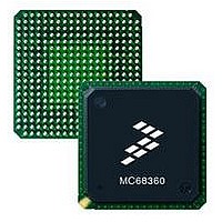
MC68360CAI25L Freescale Semiconductor, MC68360CAI25L Datasheet - Page 596

MC68360CAI25L
Manufacturer Part Number
MC68360CAI25L
Description
IC MPU QUICC 25MHZ 240-FQFP
Manufacturer
Freescale Semiconductor
Datasheets
1.MC68EN360VR25L.pdf
(14 pages)
2.MC68EN360VR25L.pdf
(2 pages)
3.MC68360AI25L.pdf
(962 pages)
4.MC68360CAI25L.pdf
(24 pages)
Specifications of MC68360CAI25L
Processor Type
M683xx 32-Bit
Speed
25MHz
Voltage
5V
Mounting Type
Surface Mount
Package / Case
240-FQFP
Family Name
M68000
Device Core
ColdFire
Device Core Size
32b
Frequency (max)
25MHz
Instruction Set Architecture
RISC
Supply Voltage 1 (typ)
5V
Operating Supply Voltage (max)
5.25V
Operating Supply Voltage (min)
4.75V
Operating Temp Range
-40C to 85C
Operating Temperature Classification
Industrial
Mounting
Surface Mount
Pin Count
240
Package Type
FQFP
Controller Family/series
68K
Core Size
32 Bit
Cpu Speed
25MHz
No. Of Timers
4
Embedded Interface Type
SCP, TDM
Digital Ic Case Style
FQFP
Supply Voltage Range
3V To 3.6V, 4.75V To 5.25V
Rohs Compliant
Yes
Lead Free Status / RoHS Status
Lead free / RoHS Compliant
Features
-
Lead Free Status / Rohs Status
Compliant
Available stocks
Company
Part Number
Manufacturer
Quantity
Price
Company:
Part Number:
MC68360CAI25L
Manufacturer:
SAMTEC
Quantity:
1 000
Company:
Part Number:
MC68360CAI25L
Manufacturer:
FREESCAL
Quantity:
717
Company:
Part Number:
MC68360CAI25L
Manufacturer:
Freescale Semiconductor
Quantity:
10 000
Part Number:
MC68360CAI25L
Manufacturer:
FREESCALE
Quantity:
20 000
- MC68EN360VR25L PDF datasheet
- MC68EN360VR25L PDF datasheet #2
- MC68360AI25L PDF datasheet #3
- MC68360CAI25L PDF datasheet #4
- Current page: 596 of 962
- Download datasheet (4Mb)
Serial Management Controllers (SMCs)
sponding channel. Furthermore, the user should not configure BD tables of two enabled
SMCs to overlap, or erratic operation will occur.
7.11.4.2 SMC FUNCTION CODE REGISTERS (RFCR, TFCR). There are four separate
function code registers for the two SMC channels: two for receive data buffers (RFCRx) and
two for transmit data buffers (TFCRx). The FC entry contains the value that the user would
like to appear on the function code pins FC3–FC0 when the associated SDMA channel
accesses memory. It also controls the byte-ordering convention to be used in the transfers.
Receive Function Code Register
Bits 7–5—Reserved
MOT—Motorola
FC3–FC0—Function Code 3–0
These bits contain the function code value used during this SDMA channel’s memory
accesses. The user should write bit FC3 with a one to identify this SDMA channel access
as a DMA-type access. Example: FC3–FC0 = 1000 (binary). Do not write the value 0111
(binary) to these bits.
Transmit Function Code Register
Bits 7–5—Reserved
7-272
This bit should be set by the user to achieve normal operation. MOT must be set if the
data buffer is located in external memory and has a 16-bit wide memory port size.
0 = DEC (and Intel) convention is used for byte ordering—swapped operation. It is also
1 = Motorola byte ordering—normal operation. It is also called big-endian byte order-
called little-endian byte ordering. The bytes stored in each buffer word are reversed
as compared to the Motorola mode.
ing. As data is received from the serial line and put into the buffer, the most signif-
icant byte of the buffer word contains data received earlier than the least significant
byte of the same buffer word.
RBASE and TBASE should contain a value that is divisible by 8.
Freescale Semiconductor, Inc.
7
7
For More Information On This Product,
—
—
6
6
MC68360 USER’S MANUAL
Go to: www.freescale.com
5
5
MOT
MOT
NOTE
4
4
3
3
2
2
FC3–FC0
FC3–FC0
1
1
0
0
Related parts for MC68360CAI25L
Image
Part Number
Description
Manufacturer
Datasheet
Request
R
Part Number:
Description:
Manufacturer:
Freescale Semiconductor, Inc
Datasheet:

Part Number:
Description:
MC68360 MC68360 Multiple Ethernet Channels on the QUICC
Manufacturer:
Motorola / Freescale Semiconductor

Part Number:
Description:
MC68360 Implementing an 8 bit Eprom for an MC68EC040-MC68360 System
Manufacturer:
Motorola / Freescale Semiconductor

Part Number:
Description:
MC68360 Interfacing the MC68060 to the MC68360
Manufacturer:
Motorola / Freescale Semiconductor

Part Number:
Description:
MC68360 MC68360 RAM Microcode Package Option Overview
Manufacturer:
Motorola / Freescale Semiconductor

Part Number:
Description:
MC68360 MC68360 CPM-CPU Interaction
Manufacturer:
Motorola / Freescale Semiconductor

Part Number:
Description:
MC68360 Interfacing SDRAM to the MC68360 QUICC Device
Manufacturer:
Motorola / Freescale Semiconductor

Part Number:
Description:
MC68360 Interfacing the QUICC to a MCM516400 (4Mx4 10-12 column-row) DRAM
Manufacturer:
Motorola / Freescale Semiconductor

Part Number:
Description:
MC68360 Interfacing the 68360 (QUICC) to T1-E1 Systems
Manufacturer:
Motorola / Freescale Semiconductor

Part Number:
Description:
MC68360 Multiple QUICC Design Concept
Manufacturer:
Motorola / Freescale Semiconductor
Part Number:
Description:
Manufacturer:
Freescale Semiconductor, Inc
Datasheet:
Part Number:
Description:
Manufacturer:
Freescale Semiconductor, Inc
Datasheet:
Part Number:
Description:
Manufacturer:
Freescale Semiconductor, Inc
Datasheet:
Part Number:
Description:
Manufacturer:
Freescale Semiconductor, Inc
Datasheet:
Part Number:
Description:
Manufacturer:
Freescale Semiconductor, Inc
Datasheet:


