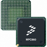
MC68360CVR25L Freescale Semiconductor, MC68360CVR25L Datasheet - Page 468

MC68360CVR25L
Manufacturer Part Number
MC68360CVR25L
Description
IC MPU QUICC 25MHZ 357-PBGA
Manufacturer
Freescale Semiconductor
Datasheets
1.MC68EN360VR25L.pdf
(14 pages)
2.MC68EN360VR25L.pdf
(2 pages)
3.MC68360AI25L.pdf
(962 pages)
Specifications of MC68360CVR25L
Processor Type
M683xx 32-Bit
Speed
25MHz
Voltage
5V
Mounting Type
Surface Mount
Package / Case
357-PBGA
Lead Free Status / RoHS Status
Lead free / RoHS Compliant
Features
-
Available stocks
Company
Part Number
Manufacturer
Quantity
Price
Company:
Part Number:
MC68360CVR25L
Manufacturer:
Freescale Semiconductor
Quantity:
10 000
Company:
Part Number:
MC68360CVR25LR2
Manufacturer:
Freescale Semiconductor
Quantity:
10 000
- Current page: 468 of 962
- Download datasheet (4Mb)
Serial Communication Controllers (SCCs)
The receiver uses a clock 8, 16, or 32 times faster then the baud rate and samples each bit
of the incoming data three times around its center. The value of the bit is determined by the
majority of those samples. If the samples do not all agree, a noise indication counter is incre-
mented. When a complete byte has been clocked in, the contents of the shift register are
transferred to the UART receive data register. If there is an error in this character, then the
appropriate error bits will be set by the CP.
The UART may receive fractional stop bits. The next character’s start bit may begin anytime
after the three middle samples have been taken.
The UART transmit shift register transmits the outgoing data on the TXDx pin. Data is
clocked synchronously with the transmit clock, which may have either an internal or external
source. The order of bit transmission is LSB first.
Only the data portion of the UART frame is actually stored in the data buffers. The start and
stop bits are always generated and stripped by the UART controller. The parity bit may also
be generated in transmission and checked during reception. Although parity is not stored in
the data buffer, its value may be inferred from the reporting mechanism in the data buffer
(i.e., character with parity errors are identified). Similarly, the optional address bit is not
stored in the transmit or receive data buffer, but is implied from the buffer descriptor itself.
Parity is generated and checked for the address bit, when present.
The RFW bit in the GSMR must be set for an 8-bit receive FIFO for the UART receiver.
7.10.16.3 SYNCHRONOUS MODE. In synchronous mode, the UART controller uses the 1
data clock for timing. The receive shift register receives the incoming data on the RXD pin
synchronously to the clock. The length and format of the serial word in bits are defined by
the control bits in the UART mode register in the same manner as for asynchronous mode.
When a complete byte has been clocked in, the contents of the shift register are transferred
to the UART receive data register. If there is an error in this character, then the appropriate
error bits will be set by the CP.
The UART transmit shift register transmits the outgoing data on the TXD pin. Data is clocked
synchronously with the transmit clock, which may have either an internal or external source.
The RFW bit in the GSMR must be set for an 8-bit receive FIFO for the UART receiver.
7-144
1. Start Bit
2. 5–8 Data Bits (LSB first)
3. Address/Data Bit (optional)
4. Parity Bit (optional)
5. Stop Bits
of the UART character is defined by the control bits in the UART mode register. The
order of reception is:
Freescale Semiconductor, Inc.
For More Information On This Product,
MC68360 USER’S MANUAL
Go to: www.freescale.com
Related parts for MC68360CVR25L
Image
Part Number
Description
Manufacturer
Datasheet
Request
R
Part Number:
Description:
Manufacturer:
Freescale Semiconductor, Inc
Datasheet:

Part Number:
Description:
MC68360 MC68360 Multiple Ethernet Channels on the QUICC
Manufacturer:
Motorola / Freescale Semiconductor

Part Number:
Description:
MC68360 Implementing an 8 bit Eprom for an MC68EC040-MC68360 System
Manufacturer:
Motorola / Freescale Semiconductor

Part Number:
Description:
MC68360 Interfacing the MC68060 to the MC68360
Manufacturer:
Motorola / Freescale Semiconductor

Part Number:
Description:
MC68360 MC68360 RAM Microcode Package Option Overview
Manufacturer:
Motorola / Freescale Semiconductor

Part Number:
Description:
MC68360 MC68360 CPM-CPU Interaction
Manufacturer:
Motorola / Freescale Semiconductor

Part Number:
Description:
MC68360 Interfacing SDRAM to the MC68360 QUICC Device
Manufacturer:
Motorola / Freescale Semiconductor

Part Number:
Description:
MC68360 Interfacing the QUICC to a MCM516400 (4Mx4 10-12 column-row) DRAM
Manufacturer:
Motorola / Freescale Semiconductor

Part Number:
Description:
MC68360 Interfacing the 68360 (QUICC) to T1-E1 Systems
Manufacturer:
Motorola / Freescale Semiconductor

Part Number:
Description:
MC68360 Multiple QUICC Design Concept
Manufacturer:
Motorola / Freescale Semiconductor
Part Number:
Description:
Manufacturer:
Freescale Semiconductor, Inc
Datasheet:
Part Number:
Description:
Manufacturer:
Freescale Semiconductor, Inc
Datasheet:
Part Number:
Description:
Manufacturer:
Freescale Semiconductor, Inc
Datasheet:
Part Number:
Description:
Manufacturer:
Freescale Semiconductor, Inc
Datasheet:
Part Number:
Description:
Manufacturer:
Freescale Semiconductor, Inc
Datasheet:


