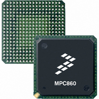
MC68360CVR25L Freescale Semiconductor, MC68360CVR25L Datasheet - Page 103

MC68360CVR25L
Manufacturer Part Number
MC68360CVR25L
Description
IC MPU QUICC 25MHZ 357-PBGA
Manufacturer
Freescale Semiconductor
Datasheets
1.MC68EN360VR25L.pdf
(14 pages)
2.MC68EN360VR25L.pdf
(2 pages)
3.MC68360AI25L.pdf
(962 pages)
Specifications of MC68360CVR25L
Processor Type
M683xx 32-Bit
Speed
25MHz
Voltage
5V
Mounting Type
Surface Mount
Package / Case
357-PBGA
Lead Free Status / RoHS Status
Lead free / RoHS Compliant
Features
-
Available stocks
Company
Part Number
Manufacturer
Quantity
Price
Company:
Part Number:
MC68360CVR25L
Manufacturer:
Freescale Semiconductor
Quantity:
10 000
Company:
Part Number:
MC68360CVR25LR2
Manufacturer:
Freescale Semiconductor
Quantity:
10 000
- Current page: 103 of 962
- Download datasheet (4Mb)
State 0—The write cycle starts in S0. During S0, the QUICC places a valid address on A31–
A0 and valid function codes on FC3–FC0. The function codes select the address space for
the cycle. The QUICC drives R/W low for a write cycle. SIZ1 and SIZ0 become valid, indi-
cating the number of bytes to be transferred.
State 1—One-half clock later during S1, the QUICC asserts AS, indicating a valid address
on the address bus. During this state, any or all of the byte write enables (WE0, WE1, WE2,
and WE3) are asserted simultaneously with AS.
State 2—During S2, the QUICC places the data to be written onto D31–D0 and samples
DSACKx at the end of S2.
FC3–FC0
DSACK0
DSACK1
A31–A2
CLKO1
D31–D0
NOTE: WE3–WE0 is not shown.
R/W
SIZ1
SIZ0
AS
DS
A0
A1
S0
LONG WORD
S2
READ
Figure 4-20. Read-Write-Read Cycles—32-Bit Port
S4
Freescale Semiconductor, Inc.
For More Information On This Product,
S0
MC68360 USER’S MANUAL
Go to: www.freescale.com
S2
WRITE
S4
S0
S2
WRITE
S4
S0
S2
READ WITH WAIT STATES
Sw
Bus Operation
Sw
S4
Related parts for MC68360CVR25L
Image
Part Number
Description
Manufacturer
Datasheet
Request
R
Part Number:
Description:
Manufacturer:
Freescale Semiconductor, Inc
Datasheet:

Part Number:
Description:
MC68360 MC68360 Multiple Ethernet Channels on the QUICC
Manufacturer:
Motorola / Freescale Semiconductor

Part Number:
Description:
MC68360 Implementing an 8 bit Eprom for an MC68EC040-MC68360 System
Manufacturer:
Motorola / Freescale Semiconductor

Part Number:
Description:
MC68360 Interfacing the MC68060 to the MC68360
Manufacturer:
Motorola / Freescale Semiconductor

Part Number:
Description:
MC68360 MC68360 RAM Microcode Package Option Overview
Manufacturer:
Motorola / Freescale Semiconductor

Part Number:
Description:
MC68360 MC68360 CPM-CPU Interaction
Manufacturer:
Motorola / Freescale Semiconductor

Part Number:
Description:
MC68360 Interfacing SDRAM to the MC68360 QUICC Device
Manufacturer:
Motorola / Freescale Semiconductor

Part Number:
Description:
MC68360 Interfacing the QUICC to a MCM516400 (4Mx4 10-12 column-row) DRAM
Manufacturer:
Motorola / Freescale Semiconductor

Part Number:
Description:
MC68360 Interfacing the 68360 (QUICC) to T1-E1 Systems
Manufacturer:
Motorola / Freescale Semiconductor

Part Number:
Description:
MC68360 Multiple QUICC Design Concept
Manufacturer:
Motorola / Freescale Semiconductor
Part Number:
Description:
Manufacturer:
Freescale Semiconductor, Inc
Datasheet:
Part Number:
Description:
Manufacturer:
Freescale Semiconductor, Inc
Datasheet:
Part Number:
Description:
Manufacturer:
Freescale Semiconductor, Inc
Datasheet:
Part Number:
Description:
Manufacturer:
Freescale Semiconductor, Inc
Datasheet:
Part Number:
Description:
Manufacturer:
Freescale Semiconductor, Inc
Datasheet:


