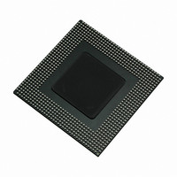
MPC8360EZUAJDGA Freescale Semiconductor, MPC8360EZUAJDGA Datasheet - Page 50

MPC8360EZUAJDGA
Manufacturer Part Number
MPC8360EZUAJDGA
Description
IC MPU POWERQUICC II PRO 740TBGA
Manufacturer
Freescale Semiconductor
Datasheet
1.MPC8360CZUAJDG.pdf
(108 pages)
Specifications of MPC8360EZUAJDGA
Processor Type
MPC83xx PowerQUICC II Pro 32-Bit
Speed
533MHz
Voltage
1.2V
Mounting Type
Surface Mount
Package / Case
740-TBGA
Processor Series
MPC8xxx
Core
e300
Data Bus Width
32 bit
Development Tools By Supplier
MPC8360E-RDK
Maximum Clock Frequency
533 MHz
Maximum Operating Temperature
+ 105 C
Mounting Style
SMD/SMT
I/o Voltage
1.8 V, 2.5 V, 3.3 V
Minimum Operating Temperature
0 C
For Use With
MPC8360EA-MDS-PB - KIT APPLICATION DEV 8360 SYSTEMMPC8360E-RDK - BOARD REFERENCE DESIGN FOR MPC
Lead Free Status / RoHS Status
Lead free / RoHS Compliant
Features
-
Lead Free Status / Rohs Status
Lead free / RoHS Compliant
Available stocks
Company
Part Number
Manufacturer
Quantity
Price
Company:
Part Number:
MPC8360EZUAJDGA
Manufacturer:
Freescale Semiconductor
Quantity:
10 000
JTAG
Figure 29
Figure 30
Figure 31
Figure 32
50
MPC8360E/MPC8358E PowerQUICC II Pro Processor Revision 2.x TBGA Silicon Hardware Specifications, Rev. 4
provides the AC test load for TDO and the boundary-scan outputs of the device.
provides the JTAG clock input timing diagram.
provides the TRST timing diagram.
provides the boundary-scan timing diagram.
External Clock
Data Outputs
Data Outputs
Data Inputs
External Clock
Boundary
Boundary
Boundary
TRST
JTAG
JTAG
Output
t
Output Data Valid
JTKLDX
Figure 29. AC Test Load for the JTAG Interface
Figure 30. JTAG Clock Input Timing Diagram
Figure 32. Boundary-Scan Timing Diagram
VM
t
JTKHKL
Figure 31. TRST Timing Diagram
VM
Z
VM
VM = Midpoint Voltage (OV DD /2)
VM = Midpoint Voltage (OV DD /2)
VM = Midpoint Voltage (OV DD /2)
t
0
JTKLDV
t
= 50 Ω
JTG
VM
t
TRST
t
JTKLDZ
t
JTDVKH
VM
R
VM
Output Data Valid
L
Data Valid
= 50 Ω
Input
t
JTGR
VM
OV
DD
t
t
JTDXKH
JTGF
/2
Freescale Semiconductor


