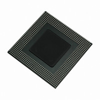
MPC8360EZUAJDGA Freescale Semiconductor, MPC8360EZUAJDGA Datasheet - Page 17

MPC8360EZUAJDGA
Manufacturer Part Number
MPC8360EZUAJDGA
Description
IC MPU POWERQUICC II PRO 740TBGA
Manufacturer
Freescale Semiconductor
Datasheet
1.MPC8360CZUAJDG.pdf
(108 pages)
Specifications of MPC8360EZUAJDGA
Processor Type
MPC83xx PowerQUICC II Pro 32-Bit
Speed
533MHz
Voltage
1.2V
Mounting Type
Surface Mount
Package / Case
740-TBGA
Processor Series
MPC8xxx
Core
e300
Data Bus Width
32 bit
Development Tools By Supplier
MPC8360E-RDK
Maximum Clock Frequency
533 MHz
Maximum Operating Temperature
+ 105 C
Mounting Style
SMD/SMT
I/o Voltage
1.8 V, 2.5 V, 3.3 V
Minimum Operating Temperature
0 C
For Use With
MPC8360EA-MDS-PB - KIT APPLICATION DEV 8360 SYSTEMMPC8360E-RDK - BOARD REFERENCE DESIGN FOR MPC
Lead Free Status / RoHS Status
Lead free / RoHS Compliant
Features
-
Lead Free Status / Rohs Status
Lead free / RoHS Compliant
Available stocks
Company
Part Number
Manufacturer
Quantity
Price
Company:
Part Number:
MPC8360EZUAJDGA
Manufacturer:
Freescale Semiconductor
Quantity:
10 000
4.3
Table 9
5
This section describes the DC and AC electrical specifications for the reset initialization timing and
electrical requirements of the MPC8360E/58E.
5.1
Table 10
Freescale Semiconductor
At recommended operating conditions with LV
GTX_CLK125 frequency
GTX_CLK125 cycle time
GTX_CLK rise and fall time
GTX_CLK125 duty cycle
GTX_CLK125 jitter
Notes:
1. Rise and fall times for GTX_CLK125 are measured from 0.5 and 2.0 V for LV
2. GTX_CLK125 is used to generate the GTX clock for the UCC Ethernet transmitter with 2% degradation. The GTX_CLK125
Input high voltage
Input low voltage
Input current
Output high voltage
Output low voltage
LV
duty cycle can be loosened from 47%/53% as long as the PHY device can tolerate the duty cycle generated by GTX_CLK.
See
and RTBI AC Timing Specifications”
MPC8360E/MPC8358E PowerQUICC II Pro Processor Revision 2.x TBGA Silicon Hardware Specifications, Rev. 4
DD
Section 8.2.2, “MII AC Timing
= 3.3 V.
RESET Initialization
provides the Gigabit reference clocks (GTX_CLK125) AC timing specifications.
provides the DC electrical characteristics for the RESET pins of the device.
Parameter/Condition
Gigabit Reference Clock Input Timing
RESET DC Electrical Characteristics
1000Base-T for RGMII & RTBI
Characteristic
LV
LV
Table 10. RESET Pins DC Electrical Characteristics
GMII & TBI
DD
DD
Table 9. GTX_CLK125 AC Timing Specifications
Specifications,”
= 2.5 V
= 3.3 V
for the duty cycle for 10Base-T and 100Base-T reference clock.
DD
= 2.5 ± 0.125 mV/ 3.3 V ± 165 mV
t
G125R
t
G125H
Symbol
t
t
G125
G125
—
Section 8.2.3, “RMII AC Timing
/t
/t
G125F
G125
Symbol
V
V
V
V
I
OH
IN
OL
IH
IL
Min
45
47
—
—
—
—
I
OH
I
OL
Condition
= –8.0 mA
= 8.0 mA
DD
—
—
—
Typical
125
= 2.5 V and from 0.6 and 2.7 V for
—
—
—
8
Specifications,” and
±150
Max
0.75
–0.3
Min
1.0
2.0
2.4
55
53
—
—
—
—
Section 8.2.5, “RGMII
OV
RESET Initialization
Unit
MHz
DD
Max
ns
ns
ps
±10
%
0.8
0.5
—
+ 0.3
Notes
Unit
—
—
1
2
2
μA
V
V
V
V
17


