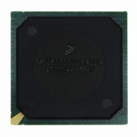
MPC8315ECVRAGDA Freescale Semiconductor, MPC8315ECVRAGDA Datasheet - Page 12

MPC8315ECVRAGDA
Manufacturer Part Number
MPC8315ECVRAGDA
Description
MPU POWERQUICC II PRO 620-PBGA
Manufacturer
Freescale Semiconductor
Datasheet
1.MPC8315VRADDA.pdf
(112 pages)
Specifications of MPC8315ECVRAGDA
Processor Type
MPC83xx PowerQUICC II Pro 32-Bit
Speed
400MHz
Voltage
1V
Mounting Type
Surface Mount
Package / Case
620-PBGA
Processor Series
MPC8xxx
Core
e300
Data Bus Width
32 bit
Maximum Clock Frequency
50 MHz
Maximum Operating Temperature
+ 105 C
Mounting Style
SMD/SMT
Minimum Operating Temperature
- 40 C
Leaded Process Compatible
Yes
Rohs Compliant
Yes
Peak Reflow Compatible (260 C)
Yes
Lead Free Status / RoHS Status
Lead free / RoHS Compliant
Features
-
Lead Free Status / Rohs Status
Lead free / RoHS Compliant
Available stocks
Company
Part Number
Manufacturer
Quantity
Price
Company:
Part Number:
MPC8315ECVRAGDA
Manufacturer:
Freescale Semiconductor
Quantity:
135
Company:
Part Number:
MPC8315ECVRAGDA
Manufacturer:
FREESCAL
Quantity:
36
Company:
Part Number:
MPC8315ECVRAGDA
Manufacturer:
Freescale Semiconductor
Quantity:
10 000
Part Number:
MPC8315ECVRAGDA
Manufacturer:
FREESCALE
Quantity:
20 000
Electrical Characteristics
3.2
The MPC8315E does not require the core supply voltage (VDD and VDDC) and I/O supply voltages
(GVDD, LVDDx_ON, LVDDx_OFF, NVDDx_ON and NVDDx_OFF) to be applied in any particular
order. During the power ramp up, before the power supplies are stable, if the I/O voltages are supplied
before the core voltage, there may be a period of time when all input and output pins be actively driven
and cause contention and/or excessive current. In order to avoid actively driving the I/O pins and to
eliminate excessive current draw, apply the continuous core voltage (VDDC) before the continuous I/O
voltages (LVDDx_ON and NVDDx_ON) and switchable core voltage (VDD) before the switchable I/O
voltages (GVDD, LVDDx_OFF, and NVDDx_OFF). PORESET should be asserted before the continuous
power supplies fully ramp up. In the case where the core voltage is applied first, the core voltage supply
must rise to 90% of its nominal value before the I/O supplies reach 0.7 V, see
supplies are stable, wait for a minimum of 32 clock cycles before negating PORESET.
The I/O power supply ramp-up slew rate should be slower than 4V/100
circuit
Figure 3
12
90%
V
.
Power sequence for continuous power supplies
1
DDR signal
DDR2 signal 1
DUART, system control, I
GPIO signals
eTSEC
shows the power-up sequencing for switchable and continuous supplies.
Output Impedance can also be adjusted through configurable options in DDR Control Driver Register
(DDRCDR). See the MPC8315E PowerQUICC II Pro Host Processor Reference Manual .
Power Sequencing
1
MPC8315E PowerQUICC
Driver Type
Continuous I/O Voltage
2
Continuous Core Voltage
C, JTAG,SPI
Table 3. Output Drive Capability (continued)
Figure 3. Power-Up Sequencing
0.7 V
t
™
II Pro Processor Hardware Specifications, Rev. 0
90%
Output Impedance
V
Power sequence for switchable power supplies
(Ω)
18
18
42
42
42
μ
s, this requirement is for ESD
Figure
LVDD = 3.3 V / 2.5 V
Switchable I/O Voltage
GVDD = 2.5 V
GVDD = 1.8 V
NVDD = 3.3 V
NVDD = 3.3 V
Switchable Core Voltage (VDD)
Voltage
Supply
3. Once all the power
Freescale Semiconductor
0.7 V
t


