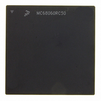
MC68060RC50 Freescale Semiconductor, MC68060RC50 Datasheet - Page 37

MC68060RC50
Manufacturer Part Number
MC68060RC50
Description
IC MPU 32BIT 50MHZ 206-PGA
Manufacturer
Freescale Semiconductor
Specifications of MC68060RC50
Processor Type
M680x0 32-Bit
Speed
50MHz
Voltage
3.3V
Mounting Type
Surface Mount
Package / Case
206-PGA
Family Name
M68000
Device Core
ColdFire
Device Core Size
32b
Frequency (max)
50MHz
Instruction Set Architecture
RISC
Supply Voltage 1 (typ)
3.3V
Operating Supply Voltage (max)
3.465V
Operating Supply Voltage (min)
3.135V
Operating Temp Range
0C to 110C
Operating Temperature Classification
Commercial
Mounting
Through Hole
Pin Count
206
Package Type
PGA
Lead Free Status / RoHS Status
Contains lead / RoHS non-compliant
Features
-
Lead Free Status / Rohs Status
Compliant
Available stocks
Company
Part Number
Manufacturer
Quantity
Price
Company:
Part Number:
MC68060RC50
Manufacturer:
MOTO
Quantity:
5 530
Company:
Part Number:
MC68060RC50C
Manufacturer:
MOTO
Quantity:
5 530
Company:
Part Number:
MC68060RC50C
Manufacturer:
MOTO
Quantity:
5 530
Company:
Part Number:
MC68060RC50C
Manufacturer:
SAMSUNG
Quantity:
5 704
- Current page: 37 of 416
- Download datasheet (2Mb)
Introduction
user distinction in the M68000 family architecture allows for the writing of application soft-
ware that executes in the user mode and migrates to the MC68060 from any M68000 family
platform without modification. The supervisor programming model contains the control fea-
tures that system designers need to modify system software when porting to a new design.
For example, only the supervisor software can read or write to the TTRs of the MC68060.
The existence of the TTRs does not affect the programming resources of user application
programs.
The user programming model includes eight data registers, seven address registers, and a
stack pointer register. The address registers and stack pointer can be used as base address
registers or software stack pointers, and any of the 16 registers can be used as index reg-
isters. Two control registers are available in the user mode—the program counter (PC),
which usually contains the address of the instruction that the MC68060 is executing, and the
lower byte of the SR, which is accessible as the condition code register (CCR). The CCR
contains the condition codes that reflect the results of a previous operation and can be used
for conditional instruction execution in a program.
The supervisor programming model includes the upper byte of the SR, which contains oper-
ation control information. The vector base register (VBR) contains the base address of the
exception vector table, which is used in exception processing. The source function code
(SFC) and destination function code (DFC) registers contain 3-bit function codes. These
function codes can be considered extensions to the 32-bit logical address. The processor
automatically generates function codes to select address spaces for data and program
accesses in the user and supervisor modes. Some instructions use the alternate function
code registers to specify the function codes for various operations.
The processor configuration register (PCR) contains bits which control the internal pipelines
of the MC68060 design.
The bus control register (BUSCR) is used to control software emulation of locked bus trans-
actions.
The cache control register (CACR) controls enabling of the on-chip instruction and data
caches of the MC68060. The supervisor root pointer (SRP) and user root pointer (URP) reg-
isters point to the root of the address translation table tree to be used for supervisor and user
mode accesses.
The translation control register (TCR) enables logical-to-physical address translation and
selects either 4- or 8-Kbyte page sizes. There are four TTRs, two for instruction accesses
and two for data accesses. These registers allow portions of the logical address space to be
transparently mapped and accessed without the use of resident descriptors in an ATC.
The user programming model can also access the entire floating-point programming model.
The eight 80-bit floating-point data registers are analogous to the integer data registers. A
32-bit floating-point control register (FPCR) contains an exception enable byte that enables
and disables traps for each class of floating-point exceptions and a mode byte that sets the
user-selectable rounding and precision modes. A floating-point status register (FPSR) con-
tains a condition code byte, quotient byte, exception status byte, and accrued exception
MOTOROLA
M68060 USER’S MANUAL
1-13
Related parts for MC68060RC50
Image
Part Number
Description
Manufacturer
Datasheet
Request
R
Part Number:
Description:
Mc68060 Superscalar 68k Microprocessor Including The Lc060 And Ec060
Manufacturer:
Freescale Semiconductor, Inc
Datasheet:
Part Number:
Description:
Manufacturer:
Freescale Semiconductor, Inc
Datasheet:
Part Number:
Description:
Manufacturer:
Freescale Semiconductor, Inc
Datasheet:
Part Number:
Description:
Manufacturer:
Freescale Semiconductor, Inc
Datasheet:
Part Number:
Description:
Manufacturer:
Freescale Semiconductor, Inc
Datasheet:
Part Number:
Description:
Manufacturer:
Freescale Semiconductor, Inc
Datasheet:
Part Number:
Description:
Manufacturer:
Freescale Semiconductor, Inc
Datasheet:
Part Number:
Description:
Manufacturer:
Freescale Semiconductor, Inc
Datasheet:
Part Number:
Description:
Manufacturer:
Freescale Semiconductor, Inc
Datasheet:
Part Number:
Description:
Manufacturer:
Freescale Semiconductor, Inc
Datasheet:
Part Number:
Description:
Manufacturer:
Freescale Semiconductor, Inc
Datasheet:
Part Number:
Description:
Manufacturer:
Freescale Semiconductor, Inc
Datasheet:
Part Number:
Description:
Manufacturer:
Freescale Semiconductor, Inc
Datasheet:
Part Number:
Description:
Manufacturer:
Freescale Semiconductor, Inc
Datasheet:
Part Number:
Description:
Manufacturer:
Freescale Semiconductor, Inc
Datasheet:


