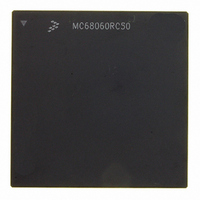
MC68060RC50 Freescale Semiconductor, MC68060RC50 Datasheet - Page 203

MC68060RC50
Manufacturer Part Number
MC68060RC50
Description
IC MPU 32BIT 50MHZ 206-PGA
Manufacturer
Freescale Semiconductor
Specifications of MC68060RC50
Processor Type
M680x0 32-Bit
Speed
50MHz
Voltage
3.3V
Mounting Type
Surface Mount
Package / Case
206-PGA
Family Name
M68000
Device Core
ColdFire
Device Core Size
32b
Frequency (max)
50MHz
Instruction Set Architecture
RISC
Supply Voltage 1 (typ)
3.3V
Operating Supply Voltage (max)
3.465V
Operating Supply Voltage (min)
3.135V
Operating Temp Range
0C to 110C
Operating Temperature Classification
Commercial
Mounting
Through Hole
Pin Count
206
Package Type
PGA
Lead Free Status / RoHS Status
Contains lead / RoHS non-compliant
Features
-
Lead Free Status / Rohs Status
Compliant
Available stocks
Company
Part Number
Manufacturer
Quantity
Price
Company:
Part Number:
MC68060RC50
Manufacturer:
MOTO
Quantity:
5 530
Company:
Part Number:
MC68060RC50C
Manufacturer:
MOTO
Quantity:
5 530
Company:
Part Number:
MC68060RC50C
Manufacturer:
MOTO
Quantity:
5 530
Company:
Part Number:
MC68060RC50C
Manufacturer:
SAMSUNG
Quantity:
5 704
- Current page: 203 of 416
- Download datasheet (2Mb)
Bus Operation
implemented with an external device that latches the write data when a bus error terminates
a write cycle.
7.9.2 Retry Operation
When an external device asserts both the TA and TEA signals during a bus cycle in the
MC68040 acknowledge termination mode or if an external device asserts TRA with TEA
negated during a bus cycle in the native-MC68060 acknowledge termination mode, the pro-
cessor enters the retry bus operation sequence. The processor terminates the bus cycle and
immediately retries the bus cycle using the same access information (address and transfer
attributes). However, if the bus cycle was a cache push operation and the bus is arbitrated
away from the MC68060 before the retry operation with a snoop access during the arbitra-
tion which invalidates the cache push, the processor does not initiate a retry operation. Fig-
ure 7-39 illustrates a functional timing diagram for a retry of a read bus transfer.
7-48
Figure 7-37. Word Write Access Bus Cycle Terminated with TEA Timing
MISCELLANEOUS
ATTRIBUTES
D31–D0
A31–A0
BCLK
SIZ0
SIZ1
R/W
TEA
SAS
TIP
TA
TS
WRITE CYCLE
C1
DRIVE
PRE
M68060 USER’S MANUAL
C2
WORD
C1
WRITE STACK
DRIVE
PRE
C2
MOTOROLA
Related parts for MC68060RC50
Image
Part Number
Description
Manufacturer
Datasheet
Request
R
Part Number:
Description:
Mc68060 Superscalar 68k Microprocessor Including The Lc060 And Ec060
Manufacturer:
Freescale Semiconductor, Inc
Datasheet:
Part Number:
Description:
Manufacturer:
Freescale Semiconductor, Inc
Datasheet:
Part Number:
Description:
Manufacturer:
Freescale Semiconductor, Inc
Datasheet:
Part Number:
Description:
Manufacturer:
Freescale Semiconductor, Inc
Datasheet:
Part Number:
Description:
Manufacturer:
Freescale Semiconductor, Inc
Datasheet:
Part Number:
Description:
Manufacturer:
Freescale Semiconductor, Inc
Datasheet:
Part Number:
Description:
Manufacturer:
Freescale Semiconductor, Inc
Datasheet:
Part Number:
Description:
Manufacturer:
Freescale Semiconductor, Inc
Datasheet:
Part Number:
Description:
Manufacturer:
Freescale Semiconductor, Inc
Datasheet:
Part Number:
Description:
Manufacturer:
Freescale Semiconductor, Inc
Datasheet:
Part Number:
Description:
Manufacturer:
Freescale Semiconductor, Inc
Datasheet:
Part Number:
Description:
Manufacturer:
Freescale Semiconductor, Inc
Datasheet:
Part Number:
Description:
Manufacturer:
Freescale Semiconductor, Inc
Datasheet:
Part Number:
Description:
Manufacturer:
Freescale Semiconductor, Inc
Datasheet:
Part Number:
Description:
Manufacturer:
Freescale Semiconductor, Inc
Datasheet:


