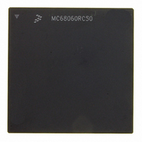
MC68060RC50 Freescale Semiconductor, MC68060RC50 Datasheet - Page 318

MC68060RC50
Manufacturer Part Number
MC68060RC50
Description
IC MPU 32BIT 50MHZ 206-PGA
Manufacturer
Freescale Semiconductor
Specifications of MC68060RC50
Processor Type
M680x0 32-Bit
Speed
50MHz
Voltage
3.3V
Mounting Type
Surface Mount
Package / Case
206-PGA
Family Name
M68000
Device Core
ColdFire
Device Core Size
32b
Frequency (max)
50MHz
Instruction Set Architecture
RISC
Supply Voltage 1 (typ)
3.3V
Operating Supply Voltage (max)
3.465V
Operating Supply Voltage (min)
3.135V
Operating Temp Range
0C to 110C
Operating Temperature Classification
Commercial
Mounting
Through Hole
Pin Count
206
Package Type
PGA
Lead Free Status / RoHS Status
Contains lead / RoHS non-compliant
Features
-
Lead Free Status / Rohs Status
Compliant
Available stocks
Company
Part Number
Manufacturer
Quantity
Price
Company:
Part Number:
MC68060RC50
Manufacturer:
MOTO
Quantity:
5 530
Company:
Part Number:
MC68060RC50C
Manufacturer:
MOTO
Quantity:
5 530
Company:
Part Number:
MC68060RC50C
Manufacturer:
MOTO
Quantity:
5 530
Company:
Part Number:
MC68060RC50C
Manufacturer:
SAMSUNG
Quantity:
5 704
- Current page: 318 of 416
- Download datasheet (2Mb)
Instruction Execution Timing
10.12 LEA, PEA, AND MOVEM EXECUTION TIMES
Table 10-20 indicates the number of clock cycles required for execution of the LEA, PEA,
and MOVEM instructions. The number of operand read and write cycles is shown in paren-
theses (r/w).
2
10.13 MULTIPRECISION INSTRUCTION EXECUTION TIMES
Table 10-21 indicates the number of clock cycles for execution of the multiprecision instruc-
tions. The number of clock cycles includes the time to fetch both operands, perform the
operations, and store the results. The number of read and write cycles is shown in paren-
theses (r/w).
10.14 STATUS REGISTER, MOVES, AND MISCELLANEOUS
Table 10-22, Table 10-23, and Table 10-24 indicate the number of clock cycles required for
execution of the status register, MOVES, and miscellaneous instructions. The number of
operand read and write cycles is shown in parentheses (r/w). Where indicated, the number
of clock cycles and r/w cycles must be added to those required for effective address calcu-
lation.
10-22
1
“n” is the number of registers being moved.
MOVEM Mem->Reg
MOVEM Reg->Mem
Add 2(1/0) cycles to the (bd,{An,PC},Xi*SF) time for a memory indirect address.
Instruction
INSTRUCTION EXECUTION TIMES
PEA
LEA
Table 10-20. LEA, PEA, and MOVEM Instruction Execution Times
Table 10-21. Multiprecision Instruction Execution Times
1
other instructions.
Where <ea>y,<ea>x is (Ay)+,(Ax)+ for CMPM and –(Ay),–(Ax) for all
1(0/0)
1(0/1)
n(0/n)
Instruction
n
(An)
2
0)
CMPM
(n/
ADDX
SUBX
ABCD
SBCD
“
“
“
(An)
n(n/
0)
—
+
-
-
(An)
n(0/
n)
–
-
-
-
M68060 USER’S MANUAL
Byte, Word
Byte, Word
Byte, Word
(d16,An)
Long
Long
Long
Size
Byte
Byte
n(n/0)
n(0/n)
1(0/0)
2(0/1)
1+n(n/0) 2+n(n/0) 1+n(n/0)
1+n(0/n) 2+n(0/n) 1+n(0/n)
(d8,An,
Xi SF)
1(0/0)
2(0/1)
op Dy,Dx
1(0/0)
1(0/0)
1(0/0)
1(0/0)
1(0/0)
1(0/0)
(bd,An,
Xi SF)
—
—
2(0/0)
3(0/1)
1
(xxx).WL (d16,PC)
1(0/0)
1(0/1)
<ea>y,<ea>x
2(2/1)
2(2/1)
2(2/0)
2(2/0)
2(2/1)
2(2/1)
2(2/1)
2(2/1)
op
1(0/0)
1(0/1)
n(n/0)
—
1
1+n(n/0) 2+n(n/0)
(d8,PC,
Xi SF)
1(0/0)
2(0/1)
—
MOTOROLA
(bd,PC,
Xi SF)
2(0/0)
2(0/1)
—
1
Related parts for MC68060RC50
Image
Part Number
Description
Manufacturer
Datasheet
Request
R
Part Number:
Description:
Mc68060 Superscalar 68k Microprocessor Including The Lc060 And Ec060
Manufacturer:
Freescale Semiconductor, Inc
Datasheet:
Part Number:
Description:
Manufacturer:
Freescale Semiconductor, Inc
Datasheet:
Part Number:
Description:
Manufacturer:
Freescale Semiconductor, Inc
Datasheet:
Part Number:
Description:
Manufacturer:
Freescale Semiconductor, Inc
Datasheet:
Part Number:
Description:
Manufacturer:
Freescale Semiconductor, Inc
Datasheet:
Part Number:
Description:
Manufacturer:
Freescale Semiconductor, Inc
Datasheet:
Part Number:
Description:
Manufacturer:
Freescale Semiconductor, Inc
Datasheet:
Part Number:
Description:
Manufacturer:
Freescale Semiconductor, Inc
Datasheet:
Part Number:
Description:
Manufacturer:
Freescale Semiconductor, Inc
Datasheet:
Part Number:
Description:
Manufacturer:
Freescale Semiconductor, Inc
Datasheet:
Part Number:
Description:
Manufacturer:
Freescale Semiconductor, Inc
Datasheet:
Part Number:
Description:
Manufacturer:
Freescale Semiconductor, Inc
Datasheet:
Part Number:
Description:
Manufacturer:
Freescale Semiconductor, Inc
Datasheet:
Part Number:
Description:
Manufacturer:
Freescale Semiconductor, Inc
Datasheet:
Part Number:
Description:
Manufacturer:
Freescale Semiconductor, Inc
Datasheet:


