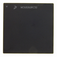
MC68060RC50 Freescale Semiconductor, MC68060RC50 Datasheet - Page 228

MC68060RC50
Manufacturer Part Number
MC68060RC50
Description
IC MPU 32BIT 50MHZ 206-PGA
Manufacturer
Freescale Semiconductor
Specifications of MC68060RC50
Processor Type
M680x0 32-Bit
Speed
50MHz
Voltage
3.3V
Mounting Type
Surface Mount
Package / Case
206-PGA
Family Name
M68000
Device Core
ColdFire
Device Core Size
32b
Frequency (max)
50MHz
Instruction Set Architecture
RISC
Supply Voltage 1 (typ)
3.3V
Operating Supply Voltage (max)
3.465V
Operating Supply Voltage (min)
3.135V
Operating Temp Range
0C to 110C
Operating Temperature Classification
Commercial
Mounting
Through Hole
Pin Count
206
Package Type
PGA
Lead Free Status / RoHS Status
Contains lead / RoHS non-compliant
Features
-
Lead Free Status / Rohs Status
Compliant
Available stocks
Company
Part Number
Manufacturer
Quantity
Price
Company:
Part Number:
MC68060RC50
Manufacturer:
MOTO
Quantity:
5 530
Company:
Part Number:
MC68060RC50C
Manufacturer:
MOTO
Quantity:
5 530
Company:
Part Number:
MC68060RC50C
Manufacturer:
MOTO
Quantity:
5 530
Company:
Part Number:
MC68060RC50C
Manufacturer:
SAMSUNG
Quantity:
5 704
- Current page: 228 of 416
- Download datasheet (2Mb)
For processor resets after the initial power-on reset, RSTI should be asserted for at least ten
BCLK periods. Figure 7-49 illustrates timings associated with a reset when the processor is
executing bus cycles. BB and TIP are negated before transitioning to a three-state level.
Resetting the processor causes any bus cycle in progress to terminate as if TEA had been
asserted. In addition, the processor initializes registers appropriately for a reset exception.
Section 8 Exception Processing describes reset exception processing. When a RESET
bus operation instruction is executed, the processor drives the reset out (RSTO) signal for
512 CLK cycles. In this case, the processor can be used to reset external devices in a sys-
tem, and the internal registers of the processor are unaffected. The external devices con-
nected to the RSTO signal are reset at the completion of the RESET instruction. An RSTI
signal that is asserted to the processor during execution of a RESET instruction immediately
resets the processor and causes the RSTO signal to negate. RSTO can be logically ANDed
with the external signal driving RSTI to derive a system reset signal that is asserted for both
an external processor reset and execution of a RESET instruction.
MOTOROLA
IPL2–IPL0
SIGNALS
D15-D0,
BCLK
RSTI
BUS
BTT
TIP
BG
TS
BR
BB
NOTE: For the processor to reset begin bus cycles after reset, BG must be asserted, TS must be negated or pulled up. BTT must be asserted (or BTT transition
from asserted to negated) eventually to indicate an end to the alternate master's tenure.
BCLK CYCLES
t 10
>
Figure 7-49. Normal Reset Timing
M68060 USER’S MANUAL
CLK CYCLES
27
Bus Operation
7-73
Related parts for MC68060RC50
Image
Part Number
Description
Manufacturer
Datasheet
Request
R
Part Number:
Description:
Mc68060 Superscalar 68k Microprocessor Including The Lc060 And Ec060
Manufacturer:
Freescale Semiconductor, Inc
Datasheet:
Part Number:
Description:
Manufacturer:
Freescale Semiconductor, Inc
Datasheet:
Part Number:
Description:
Manufacturer:
Freescale Semiconductor, Inc
Datasheet:
Part Number:
Description:
Manufacturer:
Freescale Semiconductor, Inc
Datasheet:
Part Number:
Description:
Manufacturer:
Freescale Semiconductor, Inc
Datasheet:
Part Number:
Description:
Manufacturer:
Freescale Semiconductor, Inc
Datasheet:
Part Number:
Description:
Manufacturer:
Freescale Semiconductor, Inc
Datasheet:
Part Number:
Description:
Manufacturer:
Freescale Semiconductor, Inc
Datasheet:
Part Number:
Description:
Manufacturer:
Freescale Semiconductor, Inc
Datasheet:
Part Number:
Description:
Manufacturer:
Freescale Semiconductor, Inc
Datasheet:
Part Number:
Description:
Manufacturer:
Freescale Semiconductor, Inc
Datasheet:
Part Number:
Description:
Manufacturer:
Freescale Semiconductor, Inc
Datasheet:
Part Number:
Description:
Manufacturer:
Freescale Semiconductor, Inc
Datasheet:
Part Number:
Description:
Manufacturer:
Freescale Semiconductor, Inc
Datasheet:
Part Number:
Description:
Manufacturer:
Freescale Semiconductor, Inc
Datasheet:


