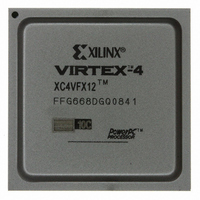
XC4VFX12-10FFG668C Xilinx Inc, XC4VFX12-10FFG668C Datasheet - Page 65

XC4VFX12-10FFG668C
Manufacturer Part Number
XC4VFX12-10FFG668C
Description
IC FPGA VIRTEX-4 FX 12K 668FCBGA
Manufacturer
Xilinx Inc
Series
Virtex™-4r
Datasheets
1.XC4VFX12-10FFG668C.pdf
(58 pages)
2.XC4VFX12-10FFG668C.pdf
(9 pages)
3.XC4VFX12-10FFG668C.pdf
(406 pages)
Specifications of XC4VFX12-10FFG668C
Total Ram Bits
663552
Number Of Logic Elements/cells
12312
Number Of Labs/clbs
1368
Number Of I /o
320
Voltage - Supply
1.14 V ~ 1.26 V
Mounting Type
Surface Mount
Operating Temperature
-40°C ~ 100°C
Package / Case
668-BBGA, FCBGA
No. Of Logic Blocks
12312
No. Of Macrocells
12312
No. Of Speed Grades
10
No. Of I/o's
320
Clock Management
DCM
I/o Supply Voltage
3.45V
Lead Free Status / RoHS Status
Lead free / RoHS Compliant
For Use With
HW-V4-ML403-UNI-G - EVALUATION PLATFORM VIRTEX-4HW-AFX-FF668-400 - BOARD DEV VIRTEX 4 FF668
Number Of Gates
-
Lead Free Status / RoHS Status
Lead free / RoHS Compliant, Lead free / RoHS Compliant
Other names
122-1591
XC4VFX12-10FFG668C
XC4VFX12-10FFG668C
Available stocks
Company
Part Number
Manufacturer
Quantity
Price
Company:
Part Number:
XC4VFX12-10FFG668C
Manufacturer:
Xilinx Inc
Quantity:
10 000
- XC4VFX12-10FFG668C PDF datasheet
- XC4VFX12-10FFG668C PDF datasheet #2
- XC4VFX12-10FFG668C PDF datasheet #3
- Current page: 65 of 406
- Download datasheet (6Mb)
DCM Attributes
Table 2-6: DCM Attributes
Virtex-4 FPGA User Guide
UG070 (v2.6) December 1, 2008
CLK_FEEDBACK
CLKDV_DIVIDE
CLKFX_DIVIDE
CLKFX_MULTIPLY
CLKIN_DIVIDE_BY_2
CLKIN_PERIOD
CLKOUT_PHASE_SHIFT
DCM Attribute Name
R
A handful of DCM attributes govern the DCM functionality.
applicable DCM attributes. This section provides a detailed description of each attribute.
For more information on applying these attributes in UCF, VHDL, or Verilog code, refer to
the Constraints Guide at:
http://www.support.xilinx.com/support/software_manuals.htm
Determines the type of feedback
applied to CLKFB.
Controls CLKDV such that the
source clock is divided by N.
This feature provides automatic
duty cycle correction such that the
CLKDV output pin has a 50/50
duty cycle always in low-frequency
mode, as well as for all integer
values of the division factor N in
high-frequency mode.
Sets the divisor (D) value of CLKFX.
The CLKFX frequency equals the
effective CLKIN frequency
multiplied by M/D.
Sets the multiply (M) of CLKFX.
The CLKFX frequency equals the
effective CLKIN frequency
multiplied by M/D.
Allows for the input clock
frequency to be divided in half
when necessary to meet the DCM
input clock frequency requirements.
Specifies the source clock period to
help the DCM adjust for optimum
CLKFX/CLKFX180 outputs.
Specifies the phase-shift mode.
Description
www.xilinx.com
String: “1X” or “NONE”
Real:
1.5, 2.0, 2.5, 3.0, 3.5, 4.0, 4.5, 5.0,
5.5, 6.0, 6.5, 7.0, 7.5, 8, 9, 10, 11,
12, 13, 14, 15, 16
Integer: 1 to 32
Integer: 2 to 32
Boolean: FALSE or TRUE
Real in ns
String: “NONE”, “FIXED”,
“VARIABLE_POSITIVE”,
“VARIABLE_CENTER”, or
“DIRECT”
Values
Table 2-6
summarizes all the
1X
2.0
1
4
FALSE
0.0
NONE
DCM Attributes
Default Value
65
Related parts for XC4VFX12-10FFG668C
Image
Part Number
Description
Manufacturer
Datasheet
Request
R

Part Number:
Description:
IC FPGA VIRTEX-4 FX 12K 363FCBGA
Manufacturer:
Xilinx Inc
Datasheet:

Part Number:
Description:
IC FPGA VIRTEX-4 FX 12K 363FCBGA
Manufacturer:
Xilinx Inc
Datasheet:

Part Number:
Description:
IC FPGA VIRTEX-4 FX 12K 363FCBGA
Manufacturer:
Xilinx Inc
Datasheet:

Part Number:
Description:
IC FPGA VIRTEX-4 FX 12K 668FCBGA
Manufacturer:
Xilinx Inc
Datasheet:

Part Number:
Description:
IC FPGA VIRTEX-4 FX 12K 363FCBGA
Manufacturer:
Xilinx Inc
Datasheet:

Part Number:
Description:
IC FPGA VIRTEX-4 FX 12K 363FCBGA
Manufacturer:
Xilinx Inc
Datasheet:

Part Number:
Description:
IC FPGA VIRTEX-4 FX 12K 668FCBGA
Manufacturer:
Xilinx Inc
Datasheet:

Part Number:
Description:
IC FPGA VIRTEX-4 FX 12K 668FCBGA
Manufacturer:
Xilinx Inc
Datasheet:

Part Number:
Description:
IC FPGA VIRTEX-4FX 363FCBGA
Manufacturer:
Xilinx Inc
Datasheet:

Part Number:
Description:
IC FPGA VIRTEX-4FX 668FFBGA
Manufacturer:
Xilinx Inc
Datasheet:

Part Number:
Description:
IC FPGA VIRTEX-4FX 363FCBGA
Manufacturer:
Xilinx Inc
Datasheet:

Part Number:
Description:
IC FPGA VIRTEX-4FX 668FFBGA
Manufacturer:
Xilinx Inc
Datasheet:

Part Number:
Description:
IC FPGA VIRTEX-4 FX 12K 668FCBGA
Manufacturer:
Xilinx Inc
Datasheet:

Part Number:
Description:
Virtex-4� Family / newest generation FPGA
Manufacturer:
XILINX [Xilinx, Inc]
Datasheet:

Part Number:
Description:
IC CPLD .8K 36MCELL 44-VQFP
Manufacturer:
Xilinx Inc
Datasheet:


