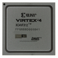
XC4VFX12-10FFG668C Xilinx Inc, XC4VFX12-10FFG668C Datasheet - Page 179

XC4VFX12-10FFG668C
Manufacturer Part Number
XC4VFX12-10FFG668C
Description
IC FPGA VIRTEX-4 FX 12K 668FCBGA
Manufacturer
Xilinx Inc
Series
Virtex™-4r
Datasheets
1.XC4VFX12-10FFG668C.pdf
(58 pages)
2.XC4VFX12-10FFG668C.pdf
(9 pages)
3.XC4VFX12-10FFG668C.pdf
(406 pages)
Specifications of XC4VFX12-10FFG668C
Total Ram Bits
663552
Number Of Logic Elements/cells
12312
Number Of Labs/clbs
1368
Number Of I /o
320
Voltage - Supply
1.14 V ~ 1.26 V
Mounting Type
Surface Mount
Operating Temperature
-40°C ~ 100°C
Package / Case
668-BBGA, FCBGA
No. Of Logic Blocks
12312
No. Of Macrocells
12312
No. Of Speed Grades
10
No. Of I/o's
320
Clock Management
DCM
I/o Supply Voltage
3.45V
Lead Free Status / RoHS Status
Lead free / RoHS Compliant
For Use With
HW-V4-ML403-UNI-G - EVALUATION PLATFORM VIRTEX-4HW-AFX-FF668-400 - BOARD DEV VIRTEX 4 FF668
Number Of Gates
-
Lead Free Status / RoHS Status
Lead free / RoHS Compliant, Lead free / RoHS Compliant
Other names
122-1591
XC4VFX12-10FFG668C
XC4VFX12-10FFG668C
Available stocks
Company
Part Number
Manufacturer
Quantity
Price
Company:
Part Number:
XC4VFX12-10FFG668C
Manufacturer:
Xilinx Inc
Quantity:
10 000
- XC4VFX12-10FFG668C PDF datasheet
- XC4VFX12-10FFG668C PDF datasheet #2
- XC4VFX12-10FFG668C PDF datasheet #3
- Current page: 179 of 406
- Download datasheet (6Mb)
Virtex-4 FPGA User Guide
UG070 (v2.6) December 1, 2008
Block RAM ECC Primitive
Block RAM ECC Port Description
R
Figure 4-35
Table 4-17
Table 4-17: Block RAM ECC Port Names and Descriptions
Notes:
1. Hamming code implemented in the block RAM ECC logic detects one of three conditions: no
WRADDR<8:0>
STATUS<1:0>
RDADDR<8:0>
detectable error, single-bit error detected and corrected on DO (but not corrected in the memory), and
double-bit error detected without correction. The result of STATUS<1:0> indicates these three
conditions.
Port Name
DO<63:0>
DI<63:0>
WRCLK
RDCLK
WREN
RDEN
SSR
lists and describes the block RAM ECC I/O port names.
shows RAMB32_S64_ECC, the block RAM ECC primitive.
Figure 4-35: RAMB32_S64_ECC: Block RAM ECC Primitive
(1)
Direction
Output
Output
Input
Input
Input
Input
Input
Input
Input
Input
www.xilinx.com
DI<63:0>
WRADDR<8:0>
RDADDR<8:0>
WREN
RDEN
S S R
WRCLK
RDCLK
Data input bus
Write address bus
Read address bus
Write enable. When WREN = 1, data will be written into
memory. When WREN = 0, write is disabled
Read enable. When RDEN = 1, data will be read from
memory. When RDEN = 0, read is disabled
Not supported when using the block RAM ECC primitive.
Always connect to GND.
Clock for write operations
Clock for read operations
Data output bus
Error status bus
RAMB32_S64_ECC
Built-in Block RAM Error Correction Code
STATUS<1:0>
DO<63:0>
Signal Description
ug070_4_ECC_022204
179
Related parts for XC4VFX12-10FFG668C
Image
Part Number
Description
Manufacturer
Datasheet
Request
R

Part Number:
Description:
IC FPGA VIRTEX-4 FX 12K 363FCBGA
Manufacturer:
Xilinx Inc
Datasheet:

Part Number:
Description:
IC FPGA VIRTEX-4 FX 12K 363FCBGA
Manufacturer:
Xilinx Inc
Datasheet:

Part Number:
Description:
IC FPGA VIRTEX-4 FX 12K 363FCBGA
Manufacturer:
Xilinx Inc
Datasheet:

Part Number:
Description:
IC FPGA VIRTEX-4 FX 12K 668FCBGA
Manufacturer:
Xilinx Inc
Datasheet:

Part Number:
Description:
IC FPGA VIRTEX-4 FX 12K 363FCBGA
Manufacturer:
Xilinx Inc
Datasheet:

Part Number:
Description:
IC FPGA VIRTEX-4 FX 12K 363FCBGA
Manufacturer:
Xilinx Inc
Datasheet:

Part Number:
Description:
IC FPGA VIRTEX-4 FX 12K 668FCBGA
Manufacturer:
Xilinx Inc
Datasheet:

Part Number:
Description:
IC FPGA VIRTEX-4 FX 12K 668FCBGA
Manufacturer:
Xilinx Inc
Datasheet:

Part Number:
Description:
IC FPGA VIRTEX-4FX 363FCBGA
Manufacturer:
Xilinx Inc
Datasheet:

Part Number:
Description:
IC FPGA VIRTEX-4FX 668FFBGA
Manufacturer:
Xilinx Inc
Datasheet:

Part Number:
Description:
IC FPGA VIRTEX-4FX 363FCBGA
Manufacturer:
Xilinx Inc
Datasheet:

Part Number:
Description:
IC FPGA VIRTEX-4FX 668FFBGA
Manufacturer:
Xilinx Inc
Datasheet:

Part Number:
Description:
IC FPGA VIRTEX-4 FX 12K 668FCBGA
Manufacturer:
Xilinx Inc
Datasheet:

Part Number:
Description:
Virtex-4� Family / newest generation FPGA
Manufacturer:
XILINX [Xilinx, Inc]
Datasheet:

Part Number:
Description:
IC CPLD .8K 36MCELL 44-VQFP
Manufacturer:
Xilinx Inc
Datasheet:


