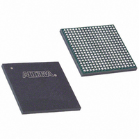
EP1C20F324C7N Altera, EP1C20F324C7N Datasheet - Page 77

EP1C20F324C7N
Manufacturer Part Number
EP1C20F324C7N
Description
IC CYCLONE FPGA 20K LE 324-FBGA
Manufacturer
Altera
Series
Cyclone®r
Datasheet
1.EP1C3T144C8.pdf
(106 pages)
Specifications of EP1C20F324C7N
Number Of Logic Elements/cells
20060
Number Of Labs/clbs
2006
Total Ram Bits
294912
Number Of I /o
233
Voltage - Supply
1.425 V ~ 1.575 V
Mounting Type
Surface Mount
Operating Temperature
0°C ~ 85°C
Package / Case
324-FBGA
Lead Free Status / RoHS Status
Lead free / RoHS Compliant
Number Of Gates
-
Other names
544-1678
Available stocks
Company
Part Number
Manufacturer
Quantity
Price
Company:
Part Number:
EP1C20F324C7N
Manufacturer:
ALTERA
Quantity:
784
Part Number:
EP1C20F324C7N
Manufacturer:
ALTERA
Quantity:
20 000
Altera Corporation
May 2008
Notes to
(1)
(2)
(3)
(4)
(5)
(6)
(7)
(8)
(9)
(10) Pin pull-up resistance values will lower if an external source drives the pin higher than V
(11) Drive strength is programmable according to values in
(12) Overdrive is possible when a 1.5 V or 1.8 V and a 2.5 V or 3.3 V input signal feeds an input pin. Turn on “Allow
(13) The Cyclone LVDS interface requires a resistor network outside of the transmitter channels.
(14) Capacitance is sample-tested only. Capacitance is measured using time-domain reflections (TDR). Measurement
C
C
C
C
C
Table 4–16. Cyclone Device Capacitance
IO
LVDS
VREF
DPCLK
CLK
Symbol
Refer to the
Conditions beyond those listed in
operation at the absolute maximum ratings for extended periods of time may have adverse affects on the device.
Minimum DC input is –0.5 V. During transitions, the inputs may undershoot to –2.0 V or overshoot to 4.6 V for
input currents less than 100 mA and periods shorter than 20 ns.
Maximum V
All pins, including dedicated inputs, clock, I/O, and JTAG pins, may be driven before V
powered.
Typical values are for T
V
This value is specified for normal device operation. The value may vary during power-up. This applies for all
V
R
will be lower if an external source drives the pin higher than V
voltage overdrive” for LVTTL/LVCMOS input pins in the Assignments > Device > Device and Pin Options > Pin
Placement tab when a device has this I/O combination. However, higher leakage current is expected.
accuracy is within ±0.5 pF.
CONF
I
CCIO
= ground, no load, no toggling inputs.
Tables 4–1
settings (3.3, 2.5, 1.8, and 1.5 V).
is the measured value of internal pull-up resistance when the I/O pin is tied directly to GND. R
Operating Requirements for Altera Devices Data
CC
Input capacitance for user I/O pin
Input capacitance for dual-purpose LVDS/user I/O pin
Input capacitance for dual-purpose V
Input capacitance for dual-purpose
Input capacitance for CLK pin.
rise time is 100 ms, and V
through 4–16:
A
= 25° C, V
Table 4–1
CCINT
Parameter
CC
= 1.5 V, and V
must rise monotonically.
may cause permanent damage to a device. Additionally, device
Note (14)
DPCLK
R E F
Cyclone Architecture
CCIO
Sheet.
/user I/O pin.
= 1.5 V, 1.8 V, 2.5 V, and 3.3 V.
/user I/O pin.
C C I O
.
chapter in the Cyclone Device Handbook.
Typical
12.0
CCINT
4.0
4.7
4.4
4.7
Operating Conditions
CCIO
.
and V
CCIO
Preliminary
CONF
are
Unit
pF
pF
pF
pF
pF
value
4–7


