EP1C20F324C7N Altera, EP1C20F324C7N Datasheet - Page 64
EP1C20F324C7N
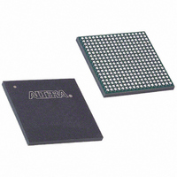
Manufacturer Part Number
EP1C20F324C7N
Description
IC CYCLONE FPGA 20K LE 324-FBGA
Manufacturer
Altera
Series
Cyclone®r
Datasheet
1.EP1C3T144C8.pdf
(106 pages)
Specifications of EP1C20F324C7N
Number Of Logic Elements/cells
20060
Number Of Labs/clbs
2006
Total Ram Bits
294912
Number Of I /o
233
Voltage - Supply
1.425 V ~ 1.575 V
Mounting Type
Surface Mount
Operating Temperature
0°C ~ 85°C
Package / Case
324-FBGA
Lead Free Status / RoHS Status
Lead free / RoHS Compliant
Number Of Gates
-
Other names
544-1678
Available stocks
Company
Part Number
Manufacturer
Quantity
Price
Company:

Part Number:
EP1C20F324C7N
Manufacturer:
ALTERA
Quantity:
784
Part Number:
EP1C20F324C7N
Manufacturer:
ALTERA
Quantity:
20 000


Cyclone Device Handbook, Volume 1
3–2
Preliminary
Note to
(1)
USERCODE
IDCODE
HIGHZ
CLAMP
ICR instructions
PULSE_NCONFIG
CONFIG_IO
SignalTap II
instructions
Table 3–1. Cyclone JTAG Instructions (Part 2 of 2)
JTAG Instruction
Bus hold and weak pull-up resistor features override the high-impedance state of HIGHZ, CLAMP, and EXTEST.
(1)
(1)
Table
3–1:
00 0000 0111
00 0000 0110
00 0000 1011
00 0000 1010
00 0000 0001
00 0000 1101
Instruction Code
In the Quartus II software, there is an Auto Usercode feature where you
can choose to use the checksum value of a programming file as the JTAG
user code. If selected, the checksum is automatically loaded to the
USERCODE register. Choose Assignments > Device > Device and Pin
Options > General. Turn on Auto Usercode.
—
—
Selects the 32-bit USERCODE register and places it between the
TDI and TDO pins, allowing the USERCODE to be serially shifted
out of TDO.
Selects the IDCODE register and places it between TDI and TDO,
allowing the IDCODE to be serially shifted out of TDO.
Places the 1-bit bypass register between the TDI and TDO pins,
which allows the BST data to pass synchronously through selected
devices to adjacent devices during normal device operation, while
tri-stating all of the I/O pins.
Places the 1-bit bypass register between the TDI and TDO pins,
which allows the BST data to pass synchronously through selected
devices to adjacent devices during normal device operation while
holding I/O pins to a state defined by the data in the boundary-scan
register.
Used when configuring a Cyclone device via the JTAG port with a
MasterBlaster
using a Jam File or Jam Byte-Code File via an embedded
processor.
Emulates pulsing the
even though the physical pin is unaffected.
Allows configuration of I/O standards through the JTAG chain for
JTAG testing. Can be executed before, after, or during
configuration. Stops configuration if executed during configuration.
Once issued, the
to reset the configuration device.
device is reconfigured.
Monitors internal device operation with the SignalTap II embedded
logic analyzer.
TM
or ByteBlasterMV
CONFIG_IO
nCONFIG
Description
instruction will hold
pin low to trigger reconfiguration
nSTATUS
TM
download cable, or when
is held low until the
Altera Corporation
nSTATUS
May 2008
low
Related parts for EP1C20F324C7N
Image
Part Number
Description
Manufacturer
Datasheet
Request
R

Part Number:
Description:
Cyclone FPGA Family
Manufacturer:
ALTERA [Altera Corporation]
Datasheet:

Part Number:
Description:
CYCLONE II STARTER KIT EP2C20N
Manufacturer:
Altera
Datasheet:


Part Number:
Description:
CPLD, EP610 Family, ECMOS Process, 300 Gates, 16 Macro Cells, 16 Reg., 16 User I/Os, 5V Supply, 35 Speed Grade, 24DIP
Manufacturer:
Altera Corporation
Datasheet:
Part Number:
Description:
CPLD, EP610 Family, ECMOS Process, 300 Gates, 16 Macro Cells, 16 Reg., 16 User I/Os, 5V Supply, 15 Speed Grade, 24DIP
Manufacturer:
Altera Corporation
Datasheet:
Part Number:
Description:
Manufacturer:
Altera Corporation
Datasheet:
Part Number:
Description:
CPLD, EP610 Family, ECMOS Process, 300 Gates, 16 Macro Cells, 16 Reg., 16 User I/Os, 5V Supply, 30 Speed Grade, 24DIP
Manufacturer:
Altera Corporation
Datasheet:
Part Number:
Description:
High-performance, low-power erasable programmable logic devices with 8 macrocells, 10ns
Manufacturer:
Altera Corporation
Datasheet:
Part Number:
Description:
High-performance, low-power erasable programmable logic devices with 8 macrocells, 7ns
Manufacturer:
Altera Corporation
Datasheet:
Part Number:
Description:
Classic EPLD
Manufacturer:
Altera Corporation
Datasheet:
Part Number:
Description:
High-performance, low-power erasable programmable logic devices with 8 macrocells, 10ns
Manufacturer:
Altera Corporation
Datasheet:
Part Number:
Description:
Manufacturer:
Altera Corporation
Datasheet:
Part Number:
Description:
Manufacturer:
Altera Corporation
Datasheet:
Part Number:
Description:
Manufacturer:
Altera Corporation
Datasheet: