EP1C20F324C7N Altera, EP1C20F324C7N Datasheet - Page 31
EP1C20F324C7N
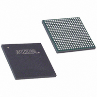
Manufacturer Part Number
EP1C20F324C7N
Description
IC CYCLONE FPGA 20K LE 324-FBGA
Manufacturer
Altera
Series
Cyclone®r
Datasheet
1.EP1C3T144C8.pdf
(106 pages)
Specifications of EP1C20F324C7N
Number Of Logic Elements/cells
20060
Number Of Labs/clbs
2006
Total Ram Bits
294912
Number Of I /o
233
Voltage - Supply
1.425 V ~ 1.575 V
Mounting Type
Surface Mount
Operating Temperature
0°C ~ 85°C
Package / Case
324-FBGA
Lead Free Status / RoHS Status
Lead free / RoHS Compliant
Number Of Gates
-
Other names
544-1678
Available stocks
Company
Part Number
Manufacturer
Quantity
Price
Company:

Part Number:
EP1C20F324C7N
Manufacturer:
ALTERA
Quantity:
784
Part Number:
EP1C20F324C7N
Manufacturer:
ALTERA
Quantity:
20 000


Figure 2–17. Independent Clock Mode
Notes to
(1)
(2)
Altera Corporation
May 2008
clken
clock
wren
A
A
A
data
byteena
address
All registers shown have asynchronous clear ports.
Violating the setup or hold time on the address registers could corrupt the memory contents. This applies to both
read and write operations.
A
[ ]
6
A
Figure
A
[ ]
[ ]
6 LAB Row Clocks
2–17:
D
ENA
D
ENA
D
ENA
D
ENA
Q
Q
Q
Q
Independent Clock Mode
The M4K memory blocks implement independent clock mode for true
dual-port memory. In this mode, a separate clock is available for each port
(ports A and B). Clock A controls all registers on the port A side, while
clock B controls all registers on the port B side. Each port, A and B, also
supports independent clock enables and asynchronous clear signals for
port A and B registers.
independent clock mode.
Input/Output Clock Mode
Input/output clock mode can be implemented for both the true and
simple dual-port memory modes. On each of the two ports, A or B, one
clock controls all registers for inputs into the memory block: data input,
wren, and address. The other clock controls the block's data output
registers. Each memory block port, A or B, also supports independent
clock enables and asynchronous clear signals for input and output
registers.
clock mode.
Generator
Write
Pulse
Figures 2–18
D
ENA
Notes
Data In
Byte Enable A
Address A
Write/Read
Enable
Data Out
Q
A
(1),
Memory Block
256 ´ 16 (2)
q
1,024 ´ 4
2,048 ´ 2
4,096 ´ 1
A
512 ´ 8
[ ]
(2)
and
q
Figure 2–17
B
[ ]
Byte Enable B
Write/Read
Address B
2–19
Data Out
Data In
Enable
B
Q
ENA
show the memory block in input/output
D
shows an M4K memory block in
Generator
Write
Pulse
Q
Q
Q
Q
ENA
ENA
ENA
ENA
D
D
D
D
Embedded Memory
Preliminary
6
data
byteena
address
wren
clken
clock
2–25
B
B
B
B
[ ]
B
B
[ ]
[ ]
Related parts for EP1C20F324C7N
Image
Part Number
Description
Manufacturer
Datasheet
Request
R

Part Number:
Description:
Cyclone FPGA Family
Manufacturer:
ALTERA [Altera Corporation]
Datasheet:

Part Number:
Description:
CYCLONE II STARTER KIT EP2C20N
Manufacturer:
Altera
Datasheet:


Part Number:
Description:
CPLD, EP610 Family, ECMOS Process, 300 Gates, 16 Macro Cells, 16 Reg., 16 User I/Os, 5V Supply, 35 Speed Grade, 24DIP
Manufacturer:
Altera Corporation
Datasheet:
Part Number:
Description:
CPLD, EP610 Family, ECMOS Process, 300 Gates, 16 Macro Cells, 16 Reg., 16 User I/Os, 5V Supply, 15 Speed Grade, 24DIP
Manufacturer:
Altera Corporation
Datasheet:
Part Number:
Description:
Manufacturer:
Altera Corporation
Datasheet:
Part Number:
Description:
CPLD, EP610 Family, ECMOS Process, 300 Gates, 16 Macro Cells, 16 Reg., 16 User I/Os, 5V Supply, 30 Speed Grade, 24DIP
Manufacturer:
Altera Corporation
Datasheet:
Part Number:
Description:
High-performance, low-power erasable programmable logic devices with 8 macrocells, 10ns
Manufacturer:
Altera Corporation
Datasheet:
Part Number:
Description:
High-performance, low-power erasable programmable logic devices with 8 macrocells, 7ns
Manufacturer:
Altera Corporation
Datasheet:
Part Number:
Description:
Classic EPLD
Manufacturer:
Altera Corporation
Datasheet:
Part Number:
Description:
High-performance, low-power erasable programmable logic devices with 8 macrocells, 10ns
Manufacturer:
Altera Corporation
Datasheet:
Part Number:
Description:
Manufacturer:
Altera Corporation
Datasheet:
Part Number:
Description:
Manufacturer:
Altera Corporation
Datasheet:
Part Number:
Description:
Manufacturer:
Altera Corporation
Datasheet: