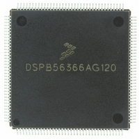
DSPB56366AG120 Freescale Semiconductor, DSPB56366AG120 Datasheet - Page 25

DSPB56366AG120
Manufacturer Part Number
DSPB56366AG120
Description
IC DSP 24BIT AUD 120MHZ 144-LQFP
Manufacturer
Freescale Semiconductor
Series
Symphony™r
Type
Audio Processorr
Datasheet
1.DSPB56366AG120.pdf
(110 pages)
Specifications of DSPB56366AG120
Interface
Host Interface, I²C, SAI, SPI
Clock Rate
120MHz
Non-volatile Memory
ROM (240 kB)
On-chip Ram
69kB
Voltage - I/o
3.30V
Voltage - Core
3.30V
Operating Temperature
-40°C ~ 110°C
Mounting Type
Surface Mount
Package / Case
144-LQFP
Lead Free Status / RoHS Status
Lead free / RoHS Compliant
Available stocks
Company
Part Number
Manufacturer
Quantity
Price
Company:
Part Number:
DSPB56366AG120
Manufacturer:
TOSHIBA
Quantity:
639
Company:
Part Number:
DSPB56366AG120
Manufacturer:
FREESCAL
Quantity:
273
Company:
Part Number:
DSPB56366AG120
Manufacturer:
Freescale Semiconductor
Quantity:
10 000
2.13
Freescale Semiconductor
Signal
Name
TDO
TMS
TCK
TDI
JTAG/OnCE Interface
Signal
Output
Type
Input
Input
Input
State during
Tri-stated
Reset
Input
Input
Input
Test Clock—TCK is a test clock input signal used to synchronize the JTAG test
logic. It has an internal pull-up resistor.
This input is 5 V tolerant.
Test Data Input—TDI is a test data serial input signal used for test instructions and
data. TDI is sampled on the rising edge of TCK and has an internal pull-up resistor.
This input is 5 V tolerant.
Test Data Output—TDO is a test data serial output signal used for test instructions
and data. TDO is tri-statable and is actively driven in the shift-IR and shift-DR
controller states. TDO changes on the falling edge of TCK.
Test Mode Select—TMS is an input signal used to sequence the test controller’s
state machine. TMS is sampled on the rising edge of TCK and has an internal
pull-up resistor.
This input is 5 V tolerant.
Table 2-15 JTAG/OnCE Interface
DSP56366 Technical Data, Rev. 3.1
Signal Description
2-21


