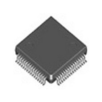
IDT82V3355TF IDT, Integrated Device Technology Inc, IDT82V3355TF Datasheet - Page 15

IDT82V3355TF
Manufacturer Part Number
IDT82V3355TF
Description
Manufacturer
IDT, Integrated Device Technology Inc
Datasheet
1.IDT82V3355TF.pdf
(135 pages)
Specifications of IDT82V3355TF
Function
Wan PLL
Operating Temperature (max)
85C
Operating Temperature (min)
-40C
Package Type
TQFP
Pin Count
64
Mounting
Surface Mount
Lead Free Status / Rohs Status
Not Compliant
Available stocks
Company
Part Number
Manufacturer
Quantity
Price
Company:
Part Number:
IDT82V3355TFG
Manufacturer:
IDT, Integrated Device Technology Inc
Quantity:
10 000
Company:
Part Number:
IDT82V3355TFG8
Manufacturer:
IDT, Integrated Device Technology Inc
Quantity:
10 000
- Current page: 15 of 135
- Download datasheet (2Mb)
Table 1: Pin Description (Continued)
Pin Description
IDT82V3355
VDD_DIFF
VDDD1
VDDD2
VDDD3
VDDD4
VDDD5
VDDD6
DGND1
DGND2
DGND3
DGND4
DGND5
DGND6
VDDA1
VDDA2
VDDA3
Name
TRST
TMS
TCK
TDO
TDI
36, 38, 39, 45, 46
Pin No.
37
41
49
51
50
12
32
54
14
57
22
11
10
31
40
53
8
9
4
7
pull-down
pull-down
Ground
pull-up
pull-up
Power
Power
Power
I/O
O
I
I
I
I
CMOS
CMOS
CMOS
CMOS
CMOS
Type
-
-
-
-
JTAG (per IEEE 1149.1)
TRST: JTAG Test Reset (Active Low)
A low signal on this pin resets the JTAG test port.
This pin should be connected to ground when JTAG is not used.
TMS: JTAG Test Mode Select
The signal on this pin controls the JTAG test performance and is sampled on the rising edge
of TCK.
TCK: JTAG Test Clock
The clock for the JTAG test is input on this pin. TDI and TMS are sampled on the rising edge
of TCK and TDO is updated on the falling edge of TCK.
If TCK is idle at a low level, all stored-state devices contained in the test logic will indefinitely
retain their state.
TDI: JTAG Test Data Input
The test data is input on this pin. It is clocked into the device on the rising edge of TCK.
TDO: JTAG Test Data Output
The test data is output on this pin. It is clocked out of the device on the falling edge of TCK.
TDO pin outputs a high impedance signal except during the process of data scanning.
This pin can indicate the interrupt of T0 selected input clock fail, as determined by the
LOS_FLAG_ON_TDO bit (b6, 0BH). Refer to
VDDDn: 3.3 V Digital Power Supply
Each VDDDn should be paralleled with ground through a 0.1 µF capacitor.
VDDAn: 3.3 V Analog Power Supply
Each VDDAn should be paralleled with ground through a 0.1 µF capacitor.
VDD_DIFF: 3.3 V Power Supply for OUT1
DGNDn: Digital Ground
Power & Ground
15
Description
SYNCHRONOUS ETHERNET WAN PLL
Chapter 3.8.1 Input Clock Validity
1
May 19, 2009
for details.
Related parts for IDT82V3355TF
Image
Part Number
Description
Manufacturer
Datasheet
Request
R

Part Number:
Description:
TRANSLATION DEVICE DPI 80-PQFP
Manufacturer:
IDT, Integrated Device Technology Inc
Datasheet:

Part Number:
Description:
IDT PART
Manufacturer:
IDT, Integrated Device Technology Inc
Datasheet:

Part Number:
Description:
IC LIU T1/E1/J1 OCTAL 256PBGA
Manufacturer:
IDT, Integrated Device Technology Inc
Datasheet:

Part Number:
Description:
IC FREQ TIMING GENERATOR 28TSSOP
Manufacturer:
IDT, Integrated Device Technology Inc
Datasheet:

Part Number:
Description:
IC CLK DVR PLL 1:10 40VFQFPN
Manufacturer:
IDT, Integrated Device Technology Inc
Datasheet:

Part Number:
Description:
IC CLK FANOUT BUFFER 1:18 32LQFP
Manufacturer:
IDT, Integrated Device Technology Inc
Datasheet:

Part Number:
Description:
IC CLK FANOUT BUFFER 1:18 32LQFP
Manufacturer:
IDT, Integrated Device Technology Inc
Datasheet:

Part Number:
Description:
IC CK505 VREG/RES 56TSSOP
Manufacturer:
IDT, Integrated Device Technology Inc
Datasheet:

Part Number:
Description:
IC SDRAM CLK DVR 1:10 48-TSSOP
Manufacturer:
IDT, Integrated Device Technology Inc
Datasheet:

Part Number:
Description:
IC CLK DVR PLL 1:10 48TSSOP
Manufacturer:
IDT, Integrated Device Technology Inc
Datasheet:

Part Number:
Description:
IC FLEXPC CLK PROGR P4 56-TSSOP
Manufacturer:
IDT, Integrated Device Technology Inc
Datasheet:

Part Number:
Description:
IC FLEXPC CLK PROGR P4 56-TSSOP
Manufacturer:
IDT, Integrated Device Technology Inc
Datasheet:

Part Number:
Description:
IC FLEXPC CLK PROGR P4 56-SSOP
Manufacturer:
IDT, Integrated Device Technology Inc
Datasheet:

Part Number:
Description:
IC PLL CLK DRIVER 2.5V 28-TSSOP
Manufacturer:
IDT, Integrated Device Technology Inc
Datasheet:

Part Number:
Description:
IC CLOCK DRIVER 2.5V 24-TSSOP
Manufacturer:
IDT, Integrated Device Technology Inc
Datasheet:


