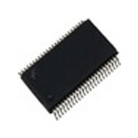
FIN1216MTDX_NL Fairchild Semiconductor, FIN1216MTDX_NL Datasheet - Page 9

FIN1216MTDX_NL
Manufacturer Part Number
FIN1216MTDX_NL
Description
Manufacturer
Fairchild Semiconductor
Datasheet
1.FIN1216MTDX_NL.pdf
(17 pages)
Specifications of FIN1216MTDX_NL
Number Of Elements
3
Number Of Receivers
3
Number Of Drivers
21
Input Type
CMOS/TTL
Operating Supply Voltage (typ)
3.3V
Differential Input High Threshold Voltage
100mV
Diff. Input Low Threshold Volt
-100mV
Output Type
Deserializer
Transmission Data Rate
4760Mbps
Operating Temp Range
-40C to 85C
Operating Temperature Classification
Industrial
Mounting
Surface Mount
Pin Count
48
Package Type
TSSOP
Lead Free Status / Rohs Status
Compliant
t
t
t
t
t
t
t
t
t
t
t
t
t
t
t
t
t
t
t
t
t
t
t
t
t
t
t
t
t
t
t
t
t
t
t
t
t
t
t
t
t
RCOL
RCOH
RSRC
RHRC
RCOP
RCOL
RCOH
RSRC
RHRC
RCOP
RCOL
RCOH
RSRC
RHRC
ROLH
ROHL
RCCD
RPDD
RSPB0
RSPB1
RSPB2
RSPB3
RSPB4
RSPB5
RSPB6
RSPB0
RSPB1
RSPB2
RSPB3
RSPB4
RSPB5
RSPB6
RSPB0
RSPB1
RSPB2
RSPB3
RSPB4
RSPB5
RSPB6
RSKM
RPLLS
Receiver AC Electrical Characteristics
Over supply voltage and operating temperatures, unless otherwise specified
Note 18: Receiver skew margin is defined as the valid sampling window after considering potential setup/hold time and minimum/maximum bit position.
Note 19: Total channel latency from serializer to deserializer is (T
Symbol
RxCLKOut LOW Time
RxCLKOut HIGH Time
RxOut Valid Prior to RxCLKOut
RxOut Valid After RxCLKOut
Receiver Clock Output (RxCLKOut) Period
RxCLKOut LOW Time
RxCLKOut HIGH Time
RxOut Valid Prior to RxCLKOut
RxOut Valid After RxCLKOut
Receiver Clock Output (RxCLKOut) Period
RxCLKOut LOW Time
RxCLKOut HIGH Time
RxOut Valid Prior to RxCLKOut
RxOut Valid After RxCLKOut
Output Rise Time (20% to 80%)
Output Fall Time (80% to 20%)
Receiver Clock Input to Clock Output Delay
Receiver Power-Down Delay
Receiver Input Strobe Position of Bit 0
Receiver Input Strobe Position of Bit 1
Receiver Input Strobe Position of Bit 2
Receiver Input Strobe Position of Bit 3
Receiver Input Strobe Position of Bit 4
Receiver Input Strobe Position of Bit 5
Receiver Input Strobe Position of Bit 6
Receiver Input Strobe Position of Bit 0
Receiver Input Strobe Position of Bit 1
Receiver Input Strobe Position of Bit 2
Receiver Input Strobe Position of Bit 3
Receiver Input Strobe Position of Bit 4
Receiver Input Strobe Position of Bit 5
Receiver Input Strobe Position of Bit 6
Receiver Input Strobe Position of Bit 0
Receiver Input Strobe Position of Bit 1
Receiver Input Strobe Position of Bit 2
Receiver Input Strobe Position of Bit 3
Receiver Input Strobe Position of Bit 4
Receiver Input Strobe Position of Bit 5
Receiver Input Strobe Position of Bit 6
RxIn Skew Margin
Receiver Phase Lock Loop Set Time
(Note 18)
Parameter
t
TCCD
)
See Figure 8
(Rising Edge Strobe)
(f
See Figure 8
(Rising Edge Strobe)
(f
See Figure 8
(Rising Edge Strobe)
(f
C
See Figure 5
See Figure 10 (Note 19)
T
See Figure 14
See Figure 17
(f
See Figure 17
(f
See Figure 17
(f
f
f
f
See Figure 18
See Figure 12
(2*T
A
L
9
40 MHz; See Figure 18
65 MHz; See Figure 18
85 MHz (FIN1218 only);
40 MHz)
65 MHz)
85 MHz) (FIN1218 only)
40 MHz)
65 MHz)
85 MHz) (FIN1218 only)
8 pF
25
Test Conditions
t
q
RCCD
C and V
). There is the clock period.
CC
3.3V
10.57
11.76
10.0
10.0
15.0
15.1
18.8
22.5
13.9
0.49
2.17
3.85
5.53
7.21
8.89
11.6
11.7
Min
490
400
252
6.5
6.0
5.0
5.0
4.5
4.0
4.5
3.5
1.0
4.5
8.1
0.7
2.9
5.1
7.3
9.5
4.0
3.5
3.5
11.0
12.2
11.6
11.6
Typ
7.8
7.3
7.7
8.4
6.3
5.4
6.3
6.5
2.2
2.1
6.9
T
T
www.fairchildsemi.com
11.27
Max
50.0
50.0
2.15
9.15
12.6
16.3
19.9
23.6
10.2
12.4
14.6
1.19
2.87
4.55
6.23
7.91
9.59
10.0
9.0
9.0
6.0
6.5
5.0
5.0
7.5
1.0
5.8
1.4
3.6
5.8
8.0
Units
ms
ns
ns
ns
ns
ns
ns
ns
ns
ns
ns
ns
ns
ns
ns
ns
P
ns
ns
ns
ns
ns
ns
ns
ns
ns
ns
ns
ns
ns
ns
ns
ns
ns
ns
ns
ns
ns
ps
ns
ns
s


