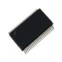
FIN1216MTDX_NL Fairchild Semiconductor, FIN1216MTDX_NL Datasheet - Page 16

FIN1216MTDX_NL
Manufacturer Part Number
FIN1216MTDX_NL
Description
Manufacturer
Fairchild Semiconductor
Datasheet
1.FIN1216MTDX_NL.pdf
(17 pages)
Specifications of FIN1216MTDX_NL
Number Of Elements
3
Number Of Receivers
3
Number Of Drivers
21
Input Type
CMOS/TTL
Operating Supply Voltage (typ)
3.3V
Differential Input High Threshold Voltage
100mV
Diff. Input Low Threshold Volt
-100mV
Output Type
Deserializer
Transmission Data Rate
4760Mbps
Operating Temp Range
-40C to 85C
Operating Temperature Classification
Industrial
Mounting
Surface Mount
Pin Count
48
Package Type
TSSOP
Lead Free Status / Rohs Status
Compliant
www.fairchildsemi.com
AC Loading and Waveforms
Note: This jitter pattern is used to test the jitter response (Clock Out) of the device over the power supply range with worst jitter
input. The specific test methodology is as follows:
•
•
Switching input data TxIn0 to TxIn20 at 0.5 MHz, and the input clock is shifted to left
CLK1 and CLK2 in Figure 11)
The
case of clock edge jump (3 ns) from graphical controllers. Cycle-to-cycle jitter at TxCLK out pin should be measured cross V
(V
CC
r
noise frequency
3ns cycle-to-cycle input jitter is the static phase error between the two clock sources. Jumping between two clock sources to simulate the worst
2 MHz).
(Continued)
FIGURE 19.
16
3ns and to the right
when data is HIGH (by switching between
CC
r
3ns (cycle-to-cycle) clock
range with 100mV noise


