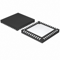
MAX11043ATL+ Maxim Integrated Products, MAX11043ATL+ Datasheet - Page 7

MAX11043ATL+
Manufacturer Part Number
MAX11043ATL+
Description
IC ADC 16BIT W/DAC 40-TQFN-EP
Manufacturer
Maxim Integrated Products
Type
ADC, DACr
Datasheet
1.MAX11043ATL.pdf
(33 pages)
Specifications of MAX11043ATL+
Resolution (bits)
16 b
Sampling Rate (per Second)
9.6M
Data Interface
Serial
Voltage Supply Source
Analog and Digital
Voltage - Supply
3 V ~ 3.6 V
Operating Temperature
-40°C ~ 125°C
Mounting Type
Surface Mount
Package / Case
40-TQFN Exposed Pad
Number Of Converters
4
Conversion Rate
1600 KSPs
Resolution
16 bit
Interface Type
SPI
Voltage Reference
2.5 V
Supply Voltage (max)
3.6 V
Supply Voltage (min)
3 V
Maximum Power Dissipation
2963 mW
Maximum Operating Temperature
+ 125 C
Mounting Style
SMD/SMT
Input Voltage
3.3 V
Minimum Operating Temperature
- 40 C
Lead Free Status / RoHS Status
Lead free / RoHS Compliant
ELECTRICAL CHARACTERISTICS (continued)
(V
V
C
OSCIN), clock divider set to 4, SHDN = DACSTEP = UP/DWN = DGND, CONVRUN = DVDD, all analog inputs driven directly through
a series 150Ω/330pF anti-alias filter, PGA gain = 1. Default filters and gain settings. DIFF = 1. T
(Note 1). Typical values are at T
Note 1: Devices 100% production tested at T
Note 2: Full scale in analog EQ mode decreases with increasing frequency at a rate of 20dB/decade from 8kHz. If digital EQ is also
Note 3: SFDR in the EQ mode is normalized to the input by subtracting the analog EQ gain at each frequency (20dB/decade) from
Note 4: The absolute input voltage range is 0 to AVDD. For optimal performance, use a common-mode voltage of AVDD/2.
Note 5: Switched capacitor input impedance is proportional to 1/fC. Where f is the sampling frequency and C is the input capacitance.
(V
T
SPI INTERFACE
SCLK Clock Period
SCLK Pulse-Width High
SCLK Pulse-Width Low
SCLK Rise to DOUT Transition
CS Fall to SCLK Rise Setup Time
SCLK Rise to CS Rise Setup Time
DIN to SCLK Rise Setup Time
DIN to SCLK Rise Hold Time
CS Pulse-Width High
CS Rise to DOUT Disable
CS Fall to DOUT Enable
EOC Fall to CS Fall
REFA
REFBP
A
AVDD
AVDD
= +25°C, unless otherwise noted.)
-1
-2
-3
-4
-5
5
4
3
2
1
0
4-Channel, 16-Bit, Simultaneous-Sampling ADCs
= V
0
= +3.0V to +3.6V, V
= C
= +3.3V, V
used, full scale decreases with increasing frequency at 40dB/decade from 5kHz.
the FFT results.
REFB
PARAMETER
with PGA, Filter, and 8-/12-Bit Dual-Stage DAC
REFA
16384
= V
INL vs. CODE
= C
REFC
CODE (LSB)
DVDD
_______________________________________________________________________________________
32768
REFB
= V
= +3.0V, f
DVDD
= C
REFD
49152
A
LP MODE
GAIN = 1
REFC
= +25°C.)
= +3.0V, C
= +2.5V (external reference), V
SCLK
SYMBOL
= C
65536
t
CSPWH
t
t
t
t
t
t
t
DOD
t
t
DOT
CSH
t
t
DOE
RDS
CSS
CH
DH
CP
CL
DS
REFD
= f
DVREG
EXCLK
-100
-120
A
-20
-40
-60
-80
= C
= +125°C. Guaranteed by design and characterization to T
0
C
C
C
0
LOAD
LOAD
LOAD
= 10µF, V
REFDAC
= 19.2MHz, V
20
40
= 20pF
= 20pF
= 20pF
60
= 1µF, f
FREQUENCY (kHz)
AGND
400ksps FFT
80
LP MODE
CONDITIONS
REFDAC
100
REFBP
= V
SCLK
120
DGND
Typical Operating Characteristics
140
, V
= V
= 38.4MHz, f
f
GAIN = 1
IN
160
REF_
REFDACH
= 50kHz
= 0V, common-mode input voltage = AVDD/2, V
180
= +2.5V, common-mode input voltage = AVDD/2,
200
= +1.25V (external reference), V
EXCLK
-100
-120
-140
A
-20
-40
-60
-80
0
= T
= 38.4MHz (external clock applied to
0
MIN
MIN
25
10
10
10
10
10
10
1
5
0
1
50
to T
100
MAX
TYP
A
FREQUENCY (kHz)
800ksps FFT
150
= -40°C.
, unless otherwise noted
LP MODE
200
MAX
250
15
20
REFDACL
300
f
GAIN = 1
IN
= 50kHz
350
UNITS
REFBP
ns
ns
ns
ns
ns
ns
ns
ns
ns
ns
ns
ns
= 0V,
400
7
=


