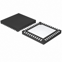
MAX11043ATL+ Maxim Integrated Products, MAX11043ATL+ Datasheet - Page 29

MAX11043ATL+
Manufacturer Part Number
MAX11043ATL+
Description
IC ADC 16BIT W/DAC 40-TQFN-EP
Manufacturer
Maxim Integrated Products
Type
ADC, DACr
Datasheet
1.MAX11043ATL.pdf
(33 pages)
Specifications of MAX11043ATL+
Resolution (bits)
16 b
Sampling Rate (per Second)
9.6M
Data Interface
Serial
Voltage Supply Source
Analog and Digital
Voltage - Supply
3 V ~ 3.6 V
Operating Temperature
-40°C ~ 125°C
Mounting Type
Surface Mount
Package / Case
40-TQFN Exposed Pad
Number Of Converters
4
Conversion Rate
1600 KSPs
Resolution
16 bit
Interface Type
SPI
Voltage Reference
2.5 V
Supply Voltage (max)
3.6 V
Supply Voltage (min)
3 V
Maximum Power Dissipation
2963 mW
Maximum Operating Temperature
+ 125 C
Mounting Style
SMD/SMT
Input Voltage
3.3 V
Minimum Operating Temperature
- 40 C
Lead Free Status / RoHS Status
Lead free / RoHS Compliant
Table 4. C-RAM and Flash Memory Map (continued)
When erasing or programming the flash, maintain the
system clock between 14MHz and 27MHz to satisfy
flash timing requirements and ensure CONVRUN = 0.
The system clock used for all digital timing is twice the
ADC sample clock (2 x EX clock/divider).
Always erase the flash page before writing new data.
The procedure for flash mass erase is as follows:
1) Read the flash mode register (18h); proceed when
2) Write 0000h to the flash address register (19h).
3) Write 60h to the flash mode register (18h).
4) Wait 200ms for erase to complete.
5) FFFFh = flash erased state.
The procedure for flash single page erase is as follows:
1) Read the flash mode register (18h); proceed when
2) Write page address, set word address to 00h in the
3) Write 40h to the flash mode register (18h).
4) Wait 20ms for page erase to complete.
5) FFFFh = flash erased state.
The procedure for flash single word write is as follows:
1) Read the flash mode register (18h); proceed when
* Recommended copy to C-RAM or flash for optimum custom-filter performance.
ADDRESS
the LSB is zero.
the LSB is zero.
flash address register (19h).
the LSB is zero.
C-RAM
3Bh
3Ch
3Dh
3Eh
3Fh
4-Channel, 16-Bit, Simultaneous-Sampling ADCs
with PGA, Filter, and 8-/12-Bit Dual-Stage DAC
ADDRESS
FLASH
Flash Erase and Programming
7Ah*
7Bh*
7Dh*
77h*
79h*
7Eh*
7Fh*
7Ch
76h
78h
______________________________________________________________________________________
ADC gain trim for gain = 32
ADC gain trim for gain = 64
LP filter coefficient -A2 for filter stage 1,
gain = 8
LP filter coefficient -A3 for filter stage 1,
gain = 8
LP filter coefficient B2 for filter stage 1,
gain = 8
MSB FOR C-RAM
—
—
—
—
—
2) Write page and word address to the flash address
3) Write the data to the flash data in register (1Ah).
4) Write 20h to the flash mode register (18h).
5) Read the flash mode register (18h); proceed when
The procedure for flash single word read is as follows:
1) Read the flash mode register (18h); proceed when
2) Write page and word address to the flash address
3) Write 80h to the flash mode register (18h).
4) Read the flash mode register (18h); proceed when
5) Read the data from the flash data out register (1Bh).
The procedure for flash to C-RAM transfer is as follows:
1) Read the flash mode register (18h); proceed when
2) Write A0h to the flash mode register (18h).
3) Read the flash mode register (18h); proceed when
4) The content of flash is transferred to C-RAM.
register (19h).
the LSB is zero (approx. 40µs).
the LSB is zero.
register (19h).
the LSB is zero (approx. 1µs).
the LSB is zero.
the LSB is zero (approx. 1ms).
Not used
Not used
LP filter gain for filter stage 1, gain = 8
Not used
LP filter coefficient B3 and rectify bit for filter stage 1,
gain = 8
LSB FOR C-RAM
—
—
—
—
—
29


