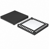
MAX11043ATL+ Maxim Integrated Products, MAX11043ATL+ Datasheet - Page 10

MAX11043ATL+
Manufacturer Part Number
MAX11043ATL+
Description
IC ADC 16BIT W/DAC 40-TQFN-EP
Manufacturer
Maxim Integrated Products
Type
ADC, DACr
Datasheet
1.MAX11043ATL.pdf
(33 pages)
Specifications of MAX11043ATL+
Resolution (bits)
16 b
Sampling Rate (per Second)
9.6M
Data Interface
Serial
Voltage Supply Source
Analog and Digital
Voltage - Supply
3 V ~ 3.6 V
Operating Temperature
-40°C ~ 125°C
Mounting Type
Surface Mount
Package / Case
40-TQFN Exposed Pad
Number Of Converters
4
Conversion Rate
1600 KSPs
Resolution
16 bit
Interface Type
SPI
Voltage Reference
2.5 V
Supply Voltage (max)
3.6 V
Supply Voltage (min)
3 V
Maximum Power Dissipation
2963 mW
Maximum Operating Temperature
+ 125 C
Mounting Style
SMD/SMT
Input Voltage
3.3 V
Minimum Operating Temperature
- 40 C
Lead Free Status / RoHS Status
Lead free / RoHS Compliant
4-Channel, 16-Bit, Simultaneous-Sampling ADCs
with PGA, Filter, and 8-/12-Bit Dual-Stage DAC
10
6, 24, 33
17, 35
5, 26
7, 23
8, 22
PIN
______________________________________________________________________________________
10
11
12
13
14
15
16
18
19
20
21
25
27
28
29
30
31
32
34
36
37
38
39
40
—
1
2
3
4
9
CONVRUN
REFDACH
DACSTEP
REFDACL
OSCOUT
UP/DWN
REFDAC
DVREG
AINBN
AINAN
OSCIN
AINDN
REFBP
AINCN
NAME
AINAP
AGND
DGND
AINDP
AINCP
AINBP
DVDD
DOUT
SHDN
AVDD
SCLK
AOUT
REFD
REFC
REFA
REFB
EOC
DIN
I.C.
CS
EP
Channel B Analog Negative Input
Channel A Reference Bypass. Bypass REFA with a nominal 1µF capacitor to AGND.
Channel A Analog Negative Input
Channel A Analog Positive Input
Analog Supply. Bypass each AVDD with a nominal 1µF capacitor to AGND.
Analog Ground. Connect AGND inputs together.
Digital Ground. Connect DGND inputs together.
Digital Supply. Bypass each DVDD with a nominal 1µF capacitor to DGND.
Regulated Digital Core Supply. Bypass DVREG to DGND with a 10µF capacitor.
DAC Step Direction Select. Drive high to step up, drive low to step down when DACSTEP is toggled.
DAC Step Input. Drive high to move the DAC output in the direction of UP/DWN on the next rising
edge of the system clock.
Convert Run. Drive high to start continuous conversions on all 4 channels. The device is idle when
CONVRUN is low.
Active-Low Serial-Interface Chip Select
Serial-Interface Data Out. Data transitions on the rising edge of SCLK.
Serial-Interface Data In. Data is sampled on the rising edge of SCLK.
Serial-Interface Clock
Internally Connected. Connect to either AGND or DGND.
Active-Low End-of-Conversion Indicator. EOC asserts low to indicate that new data is ready.
Crystal Oscillator/External Clock Input
Crystal-Oscillator Output. Leave unconnected when using external clock.
Active-High Shutdown Input. Drive high to shut down the MAX11043.
Buffered 12-Bit Fine DAC Output
Fine DAC Low Reference Bypass. Bypass REFDACL with a nominal 1µF capacitor to AGND.
Fine DAC High Reference Bypass. Bypass REFDACH with a nominal 1µF capacitor to AGND.
Coarse DAC Reference Bypass. Bypass REFDAC with a nominal 1µF capacitor to AGND.
Channel D Reference Bypass. Bypass REFD with a nominal 1µF capacitor to AGND.
Channel D Analog Negative Input
Channel D Analog Positive Input
Main Reference Bypass. Bypass REFBP with a nominal 1µF capacitor to AGND.
Channel C Analog Negative Input
Channel C Analog Positive Input
Channel C Reference Bypass. Bypass REFC with a nominal 1µF capacitor to AGND.
Channel B Reference Bypass. Bypass REFB with a nominal 1µF capacitor to AGND.
Channel B Analog Positive Input
Exposed Pad. Connect EP to a ground plane on the PCB to enhance thermal dissipation. Internally
connected to AGND. Not intended as an electrical connection point.
FUNCTION
Pin Description


