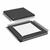
AD9271BSVZRL-25 Analog Devices Inc, AD9271BSVZRL-25 Datasheet - Page 5

AD9271BSVZRL-25
Manufacturer Part Number
AD9271BSVZRL-25
Description
IC ADC OCT 12BIT 25MSPS 100-TQFP
Manufacturer
Analog Devices Inc
Datasheet
1.AD9271BSVZ-50.pdf
(60 pages)
Specifications of AD9271BSVZRL-25
Number Of Bits
12
Sampling Rate (per Second)
25M
Data Interface
Serial, SPI™
Number Of Converters
8
Power Dissipation (max)
1.06W
Voltage Supply Source
Single Supply
Operating Temperature
-40°C ~ 85°C
Mounting Type
Surface Mount
Package / Case
100-TQFP Exposed Pad
Power Dissipation Pd
150mW
Peak Reflow Compatible (260 C)
Yes
Supply Voltage
1.8V
Sample Rate
25 MSPS
Termination Type
SMD
Supply Voltage Max
1.9V
Input Channels Per Adc
8
Lead Free Status / RoHS Status
Lead free / RoHS Compliant
For Use With
AD9271-50EBZ - BOARD EVALUATION AD9271 50MSPS
Lead Free Status / RoHS Status
Lead free / RoHS Compliant, Lead free / RoHS Compliant
Available stocks
Company
Part Number
Manufacturer
Quantity
Price
Company:
Part Number:
AD9271BSVZRL-25
Manufacturer:
AD
Quantity:
1 140
Company:
Part Number:
AD9271BSVZRL-25
Manufacturer:
Analog Devices Inc
Quantity:
10 000
Parameter
GAIN ACCURACY
GAIN CONTROL
CW DOPPLER MODE
Harmonic Distortion
Two-Tone IMD3
Channel-to-Channel
Channel-to-Channel
Overload Recovery
Gain Law Confor-
Linear Gain Error
Channel-to-Channel
INTERFACE
Normal Operating
Gain Range
Scale Factor
Response Time
Transconductance
Common Mode
Input-Referred Noise
Output DC Bias
Maximum Output
Second Harmonic
Second Harmonic
Third Harmonic
Third Harmonic
(2 × F1 − F2)
Distortion
f
at −7 dBFS,
f
at −7 dBFS
Crosstalk
Crosstalk (Over-
range Condition)
mance Error
Matching
Range
Voltage
Swing
IN1
IN2
f
at −7 dBFS
f
at −1 dBFS
f
at −7 dBFS
f
at −1 dBFS
= 5.0 MHz
= 6.0 MHz
IN
IN
IN
IN
= 5 MHz
= 5 MHz
= 5 MHz
= 5 MHz
1
3
Conditions
V
V
V
V
V
Full TGC path,
f
gain = 0 V to 1 V
25°C
0 < V
0.1 V < V
0.9 V < V
V
normalized for ideal
AAF loss
0.1 V < V
0 V to 1 V, normalized
for ideal AAF loss
30 dB change
LNA gain = 5/6/8
CW Doppler
output pins
LNA gain = 5/6/8,
R
Per channel
Per channel
IN
GAIN
GAIN
GAIN
GAIN
GAIN
GAIN
S
= 1 MHz to 10 MHz,
= 0 Ω, RFB = ∞
GAIN
= 0.5 V,
= 0 V
= 1 V
= 0 V
= 1 V
= 1 V
GAIN
GAIN
< 0.1 V
GAIN
< 0.9 V
< 0.9 V
< 1 V
Min
−1.2
−1.3
0
1.5
−73
−80
−81
−65
−54.6
−70
−70
5
+0.8
−1.2
0.2
10 to 40
31.6
350
10/12/16
1.8 /1.7/1.5
2.4
±2
Typ
AD9271-25
Rev. B | Page 5 of 60
+1.2
+1.3
1
3.6
Max
Min
−1.2
−1.3
0
1.5
Typ
−71
−72
−77
−63
−63.4
−70
−70
5
+0.8
−1.2
0.2
10 to 40
31.6
350
10/12/16
1.7 /1.5/1.4
2.4
±2
AD9271-40
Max
+1.2
+1.3
1
3.6
Min
−1.2
−1.3
0
1.5
Typ
−71
−68
−74
−66
−68.5
−70
−70
5
+0.8
−1.2
0.2
10 to 40
31.6
350
10/12/16
1.7 /1.5/1.3
2.4
±2
AD9271-50
Max
+1.2
+1.3
1
3.6
AD9271
ns
nV/√Hz
mA
mA p-p
Unit
dBFS
dBFS
dBFS
dBFS
dBc
dB
dB
Degrees
dB
dB
dB
dB
dB
V
dB
dB/V
mA/V
V


